This thread has been locked.

If you have a related question, please click the "Ask a related question" button in the top right corner. The newly created question will be automatically linked to this question.

CC2640: PCB Antenna design verification AN043

Part Number: CC2640

All,

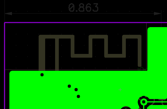
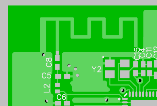
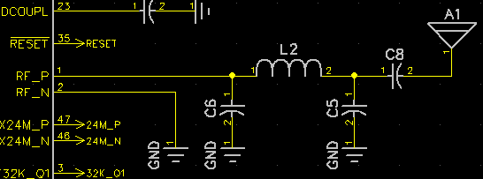
I have never designed a PCB before so having someone review my work before I send it to be assembled would be extremely helpful.  Specifically, I am a little worried about getting the PCB antenna right.  I used the application note AN043 for my design, and for the antenna matching I used the single-ended design also recommended by TI.  Below are a few screenshots of what I have so far.  Let me know if I am missing anything blatantly obvious or have anywhere that is prone to error.  Also, when assembled, not only will the PCB be in a plastic case, but a battery holder will be placed on the bottom side of the PCB, partially shadowing the antenna.  I recognize this will alter the radiation pattern, but will it alter it so severely that I won't be able to TX/RX 1 meter away?

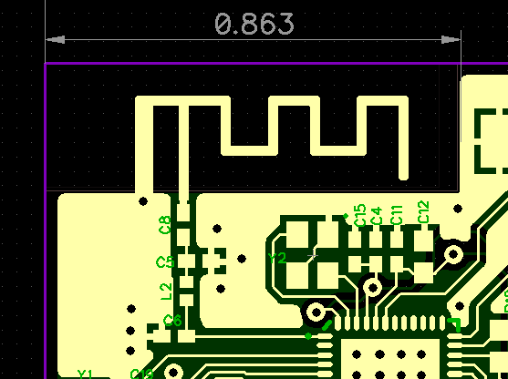
PCB Copper Top (Gold):

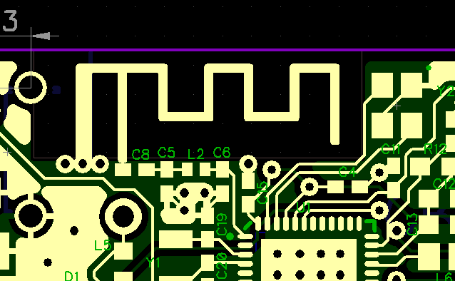
PCB Copper Bottom (Green):

3D Rendering of board:

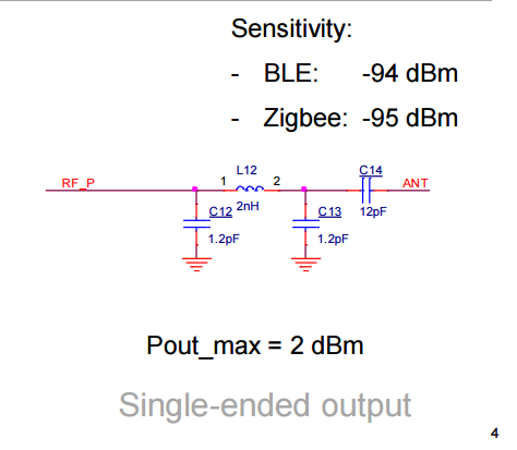
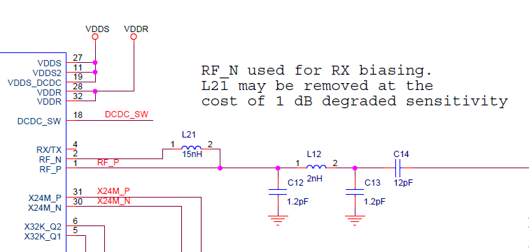
Single-ended RF design:

Let me know what I need to clarify.  Thanks!

  • Hi Cameron,

    You should have more clearance to the right of the antenna. At least 5 mm, but more is better. Having a coin cell battery partly covering the antenna will severely affect the antenna efficiency. You should still reach > 1 m without a problem though.

    There are some other issues with you design, for example the RF matching components should be placed as close to the CC2640 as possible (as in our reference designs). And why have you grounded RF-N? Please refer to these documents for details:

    processors.wiki.ti.com/.../CC26xx_HW_training_Layout_Considerations.pdf
    processors.wiki.ti.com/.../CC26xx_HW_Checklist

    Cheers,
    Fredrik
  • Fredrik,

    As always, thanks so much for the quick response.  You have been wonderful help with my other posted questions so far.

    I will add more clearance to the right side of the antenna, and I will also move the RF components closer to the CC2640, like you suggested.

    For my RF layout, I was attempting to use the single-ended design shown below:

    I found this design in this document on the wiki: RF Antennas and frontends

    I guess this design doesn't really specify what to do with RF_N, so I ended up grounding it without much thought.  Should I leave it floating instead?

    Thanks,

    Cameron

  • Hi Cameron,

    You are welcome!

    You should follow the layout in this reference design for single ended operation: www.ti.com/.../cc2650em-4xs-rd

    Regards,
    Fredrik
  • Fredrik,

    Thanks for pointing me in the direction of that schematic for single ended operation.  Based on the that schematic (image below), you can remove L21 for the cost of 1 dB degraded sensitivity.  Because of my size constraints, I decided to leave L21 out of my design and let RF_N float.  I am designing two boards that I plan to have communicate via bluetooth using this antenna design.

    After mimicking this design, and following the Application note AN043, as well as your suggested design documents, I came up with the following two boards:

    As you can see, one is much cleaner than the other, but I am hoping the design will work, even if the signal sensitivity is low (I only need to TX/RX 1 meter distance).

    I am hoping to send these boards for fabrication ASAP.  Let me know if I made any glaring mistakes.

    Thanks,

    Cameron

  • Hi Cameron,

    As I wrote in my first reply, the RF matching must be placed closer to the CC2640. You can look at this reference design for layout guidelines: www.ti.com/.../cc2650em-4xs-rd .

    In the uppermost design you should place a decoupling cap close to pin 48. Additionally you could move the antenna further to the left to get even more spacing on the right side. Ideally you should place a matching network for antenna impedance matching close to the antenna, but it you only need a few meters you do not really need it.

    The lowermost design is a bit more messy :-) Same comments as above applies here to. Additionally, there should be more clearance for the antenna, the crystal should preferably be placed closer to the IC, an the signal trace that splits the ground plane between the IC and the antenna is a big no-no.

    Cheers,
    Fredrik