This thread has been locked.

If you have a related question, please click the "Ask a related question" button in the top right corner. The newly created question will be automatically linked to this question.

CC2541EM-RD: CC2541F256RHAR

Part Number: CC2541EM-RD
Other Parts Discussed in Thread: CC2541

Hi all,

I am working on design CC2541 and  AN043 PCB antenna. I'm doing bluetooth design for the first time.

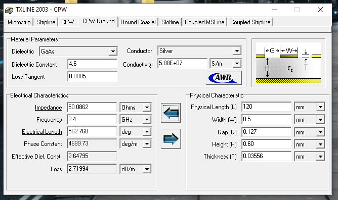
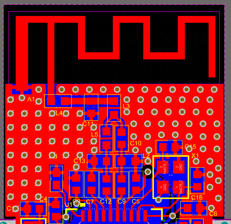
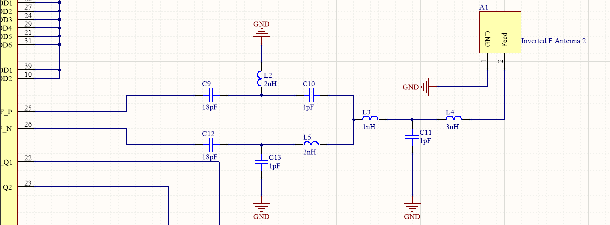
I used EM reference Design and AN043 as a reference design. I used TXLINE 2003 for the 50 ohm impedance calculation. I share the layout and calculation of the 50 ohm impedance.

Because the cost and the small board is important for AN043 and I did 2 layer board design. I set all the pins to pinout. 

Your comments about layout are very important to me. If it is missing or wrong, I will correct it and send it to produce.

Last question, How do I access the chip with pinouts except cc debugger? any suggestions??

  • I'm not fully sure what you ask about.

    - Based on the screenshot it's not possible to see if you have followed the measurements given in http://www.ti.com/lit/an/swra117d/swra117d.pdf

    - "Last question, How do I access the chip with pinouts except cc debugger": Could you rephrase the question some, not sure if I understand what you ask about. Do you want to debug/ flash  the chip with a different debugger than CCDebugger? 

  • I don't think there will be a problem with the antenna dimensions, because I have drawn the lengths exactly as AN043.

    I did the 50 ohm impedance calculation, the lengths appear on the screen, is this appropriate? Is there anything I missed?

    When we say different debugger; I debug with the FTDI converter to HM-10 (cc2541). (Accessing via the required pins.) If I wanted to do this for the board I designed, can I?

    Otherwise should I get the CC debugger?

    If we look at the general schematic and layout, is there anything that needs to be corrected and added?

  • - The trace is fairly short meaning that it will not behave like a transmission line. The width you have used is fine. 

    - I'm not familiar with debugging this device using FTDI but as long as the protocol described in "Debug Interface" in the UserGUide it should be possible. If you want to TIs software tools to debug/ flash the device you are most likely safer to use CCDebugger. 

    If C6 is a decoupling cap you have to look into the ground return path to chip ground since it looks like a trace block the routing. 

  • - Would you recommend me to make the trace longer?

    -Just in case, I'm gonna get a CC debugger.

    -Yes, C6 cap is decoupling cap and I didn't well understand what you said, can you help me do what? I've attached the ground into bottom layer, could you check please?

  • Decoupling: See 4.4 in http://www.ti.com/lit/an/swra640c/swra640c.pdf for more details.

    Trace: No, no point of having a longer trace. 

  • Hello again,

    I am curious about something else that i should know the details for CC2541F256RHAR. Could this module be used to activate a MOSFET via digital pinout without using any microcontroller? For example:

    Bluetooth should be in sleep mode when not any connection. After the connection, the module would active a digital pin to active MOSFET.

    Could you please inform me about that situation?

    Sincerely,

    M. Eyup Arslan

  • Hi Eyup,

    Yes you can wake up the device and use it to drive a pin while BLE is not actively transmitting or receiving.