Hi there,
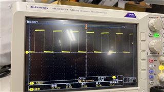
I would like to use clkin (external clock, P1.4) to be the source of ACLK
External clock is a 32.768KHz.
But it seems not work. It is always 64kHz
Do I just miss something?
void DeviceInit(void)
{
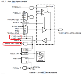
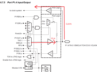
// Disable JTAG
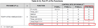
	P1SEL1 = 0x00; //P1.6 = 0
	P1SEL0 = 0x00; //P1.6 = 0
P1REN = 0;
RFPMMCTL0 = RFPMMCTL0EN_VFREG_BATSWITCH_VDOUB;
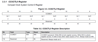
CCSCTL0 = CCSKEY; // Unlock CCS
CCSCTL6 = 0x00;
CCSCTL1 = 0; // do not half the clock speed
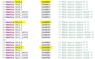
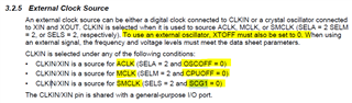
CCSCTL4 = SELA_2 + SELM_0 + SELS_0;
CCSCTL5 = DIVA_2 + DIVM_1 + DIVS_1; // Set the Dividers for ACLK (4), MCLK, and SMCLK to 1
CCSCTL8 = ACLKREQEN + MCLKREQEN + SMCLKREQEN; //disable clocks if they are not being used
TA0CCTL0 = CCIE; // Timer A0 Capture/compare interrupt enable
TA0CTL = TASSEL__ACLK + // Timer_A clock source select -> ACLK
MC_1 + // Mode control, Timer counts up to the value stored in TA0CCR0
ID_3; // Input divider -> 1/2 (4MHz/2 = 2MHz) - this is the frequency which goes to comparison register
TA0CCR0 = 1590;
CCSCTL0_H |= 0xFF; // Lock CCS
P1DIR |= 0x04; // P1.2 output
return;
}