This thread has been locked.

If you have a related question, please click the "Ask a related question" button in the top right corner. The newly created question will be automatically linked to this question.

CC1190: CC1352P1 + CC1190 issue

Part Number: CC1190
Other Parts Discussed in Thread: CC1352P, , CC1310

Hi,

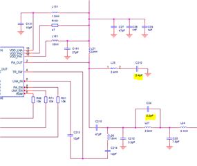
I want to boost the TX power of a CC1352P to 27dbm. I made a pcb according to the application notes and examples of this booster. However, while  CC1352P outputs the correct power e.g. 14dbm the booster's output is -30dbm. During the first tests, there wasn't any signal at the output of the booster. After many trials, I found with the oscilloscope, that every time PA is enabled, the voltage at pin VDD_PA2 was dropping to 0, because it is connected to the 3.3v bus through a 47Ohms, as in the schematic. As soon as I replaced the 47Ohm resistor, R151, with a zeroOhm resistor, it started working, but more as attenuator than as booster. In SWRA542, all power pins are connected to 3.3VC, without any resistor in series. The only difference of my pcb , is that I replaced  all 0 value components with tracks. Thus PA_IN is connected directly to LNA_OUT. Pcb layout is very similar to the proposed and all components are identical. All RF measurements are done with a Regol RSA310 spectrum analyzer. 

Thanks

  • Hi,

    Can you send your schematic ?

    Have you compared the CC1190 section with the following schematic/ref design: https://www.ti.com/lit/zip/swrc338 This is based upon the CC1310 CC1190 but the CC1190 section should be similar in your design when connected to the low power output of the sub-1 section of CC1352P.

    Which frequency are you operating at ?

    There are some filter notches in the CC1190 filter network but this should mainly effect the levels of the 2nd and 3rd harmonics if they are incorrect.

  • Thank you for your reply. The schematic is exactly the same as of the cc1310-cc1190 or SWRA477. It operates at 869.525MHz. The pcb also is almost the same with the same layer stack. I don't understand the 47 Ohms resistor at PA2. If used, it doesn't work at all. If replaced with 0 Ohm, it is working but not as expected. What's the reason of 2 power supply pins?

  • Now I'm looking better at your pcb, the only difference is that the top ground plane below the cc1190 is not the same top ground plane, but it is isolated and connected to the top ground plane with few tracks. Could this be the cause of the very reduced TX power?

  • Why have an isolated GND plane underneath the CC1190 and just connected with a few tracks ??

    I'm always dubious about having isolated GND planes and connecting them together at strategic locations since this sometimes can cause more issues then it helps. We normally prefer just to have one solid GND plane on layer 2 for a 4-layer design. Isolated GND planes or not, can be a long academic discussion but we prefer to have just one solid GND plane. 

    Can you connect the GND planes together to see if this is a route cause ?

    The two power pins feed the cascode section of the PA design.

  • I do have a solid ground plane. I'm just wondering if this could be the cause of the malfunction. 

  • The schematic looks OK. 

    When you have 10 dBm into CC1190 at the PA_IN. What conducted output power (remove antenna connection) do you measure when the PA_EN is high and (HGM is also high) ?

    Can you measure on the VDD pins of CC1190 to see if you have the expected voltage there ? The current for the PA at 27 dBm should be around 300 mA-ish so just make sure there is no voltage drop occurring.

  • Another test to debug is to remove the frond-end filtering by removing C215 and measure the output power at PA_OUT. The output match will be incorrect and there will be a natural lower output power at 50 ohm but let me know which output power you measure?

  • Feeding 10dbm to cc1190 results in -20dbm at the antenna, connected directly to the spectrum analyzer. I  checked the voltage at the pins of CC1190 and there is indeed a some ripple. I connected 3.6V directly to the power pins, with a ripple of few mV and the output was increased by 2-3dbm only. 

  • Removing C215, with  2dbm at the input, I get 10.5dbm at PA_OUT. I don't have a rf probe, thus measurement is not precise as when I connect the antenna. Nevertheless, now it seems to be kind of working. Could be a problem of the output impedance matching? I used the same components as in your app notes.

  • It sounds like the output impedance match is causing the main degradation here based upon the removal of C215 test. 

    Are you using 0402 or 0201 components ?

  • Hi, we are using 0402 components, but we asked from a Chinese company to fabricate sample pcbs and assemble all passive components. Working with RF, quality of these components is crucial. I'm waiting a reply from them about the quality and possibly specs of the components. I'm not really sure that they are MURATA or other well known manufacturer. I'll try to replace on at least one device  the passive components with MURATA originals as in TI's app notes and let you know. Thank you!

  • Hi,

    You could also try and to tweek the harmonic notches to give some indication where the main load mismatch is. If the layout is different from the reference design and also a different vendor of inductors then the filtering notches will be different and the load match will be effected. You could also try to try a few larger and smaller values of C210 & C24 to tune the notches better for your particular design. Measure the output power and the 2nd and 3rd conducted harmonics when trying new passive values.

  • Hi,

    I tried new, MURATA components and now it's working fine!!. Thank you very much for your support. Your suggestion to disconnect C215 and measure output before the matching network, saved me several days of trial and error. I'll check also the notch filters tuning. THANKS