


Other Parts Discussed in Thread: TEST2
Hello Team,
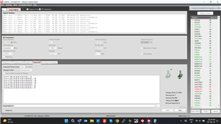
I am working on a project where I have used a cc1101 chip for RF communication.I am facing an issue, where I can send the data but am not able to receive the data on another cc1101 chip.I am sharing my register configuration and sending and receiving register functionality for reference.
- Register configuration
/CC1101 CONFIG REGSITER
#define CC1101_IOCFG2       0x00        // GDO2 output pin configuration
#define CC1101_IOCFG1       0x01        // GDO1 output pin configuration
#define CC1101_IOCFG0       0x02        // GDO0 output pin configuration
#define CC1101_FIFOTHR      0x03        // RX FIFO and TX FIFO thresholds
#define CC1101_SYNC1        0x04        // Sync word, high INT8U
#define CC1101_SYNC0        0x05        // Sync word, low INT8U
#define CC1101_PKTLEN       0x06        // Packet length
#define CC1101_PKTCTRL1     0x07        // Packet automation control
#define CC1101_PKTCTRL0     0x08        // Packet automation control
#define CC1101_ADDR         0x09        // Device address
#define CC1101_CHANNR       0x0A        // Channel number
#define CC1101_FSCTRL1      0x0B        // Frequency synthesizer control
#define CC1101_FSCTRL0      0x0C        // Frequency synthesizer control
#define CC1101_FREQ2        0x0D        // Frequency control word, high INT8U
#define CC1101_FREQ1        0x0E        // Frequency control word, middle INT8U
#define CC1101_FREQ0        0x0F        // Frequency control word, low INT8U
#define CC1101_MDMCFG4      0x10        // Modem configuration
#define CC1101_MDMCFG3      0x11        // Modem configuration
#define CC1101_MDMCFG2      0x12        // Modem configuration
#define CC1101_MDMCFG1      0x13        // Modem configuration
#define CC1101_MDMCFG0      0x14        // Modem configuration
#define CC1101_DEVIATN      0x15        // Modem deviation setting
#define CC1101_MCSM2        0x16        // Main Radio Control State Machine configuration
#define CC1101_MCSM1        0x17        // Main Radio Control State Machine configuration
#define CC1101_MCSM0        0x18        // Main Radio Control State Machine configuration
#define CC1101_FOCCFG       0x19        // Frequency Offset Compensation configuration
#define CC1101_BSCFG        0x1A        // Bit Synchronization configuration
#define CC1101_AGCCTRL2     0x1B        // AGC control
#define CC1101_AGCCTRL1     0x1C        // AGC control
#define CC1101_AGCCTRL0     0x1D        // AGC control
#define CC1101_WOREVT1      0x1E        // High INT8U Event 0 timeout
#define CC1101_WOREVT0      0x1F        // Low INT8U Event 0 timeout
#define CC1101_WORCTRL      0x20        // Wake On Radio control
#define CC1101_FREND1       0x21        // Front end RX configuration
#define CC1101_FREND0       0x22        // Front end TX configuration
#define CC1101_FSCAL3       0x23        // Frequency synthesizer calibration
#define CC1101_FSCAL2       0x24        // Frequency synthesizer calibration
#define CC1101_FSCAL1       0x25        // Frequency synthesizer calibration
#define CC1101_FSCAL0       0x26        // Frequency synthesizer calibration
#define CC1101_RCCTRL1      0x27        // RC oscillator configuration
#define CC1101_RCCTRL0      0x28        // RC oscillator configuration
#define CC1101_FSTEST       0x29        // Frequency synthesizer calibration control
#define CC1101_PTEST        0x2A        // Production test
#define CC1101_AGCTEST      0x2B        // AGC test
#define CC1101_TEST2        0x2C        // Various test settings
#define CC1101_TEST1        0x2D        // Various test settings
#define CC1101_TEST0        0x2E        // Various test settings
- Registers Value
#define VAL_IOCFG2        0x29
#define VAL_IOCFG1        0x2E
#define VAL_IOCFG0        0x06
#define VAL_FIFOTHR       0x47
#define VAL_SYNC1         0xD3
#define VAL_SYNC0         0x91
#define VAL_PKTLEN        0xFF
#define VAL_PKTCTRL1      0x04
#define VAL_PKTCTRL0      0x05
#define VAL_ADDR          0x00
#define VAL_CHANNR        0x00
#define VAL_FSCTRL1       0x06
#define VAL_FSCTRL0       0x00
#define VAL_FREQ2         0x10
#define VAL_FREQ1         0xA7
#define VAL_FREQ0         0x62
#define VAL_MDMCFG4       0xF5
#define VAL_MDMCFG3       0x83
#define VAL_MDMCFG2       0x13
#define VAL_MDMCFG1       0x22
#define VAL_MDMCFG0       0xF8
#define VAL_DEVIATN       0x15
#define VAL_MCSM2         0x07
#define VAL_MCSM1         0x33//0x3B
#define VAL_MCSM0         0x10
#define VAL_FOCCFG        0x16
#define VAL_BSCFG         0x6C
#define VAL_AGCCTRL2      0x03
#define VAL_AGCCTRL1      0x40
#define VAL_AGCCTRL0      0x91
#define VAL_WOREVT1       0x80
#define VAL_WOREVT0       0x00
#define VAL_WORCTRL       0xFB
#define VAL_FREND1        0x56
#define VAL_FREND0        0x10
#define VAL_FSCAL3        0xE9
#define VAL_FSCAL2        0x2A
#define VAL_FSCAL1        0x00
#define VAL_FSCAL0        0x1F
#define VAL_FSTEST        0x59
#define VAL_PTEST         0x7F
#define VAL_AGCTEST       0x3F
#define VAL_TEST2         0x81
#define VAL_TEST1         0x35
#define VAL_TEST0         0x09
#define VAL_PARTNUM       0x00
#define VAL_VERSION       0x06
#define VAL_FREQEST       0x00
#define VAL_LQI           0x00
#define VAL_RSSI          0x00
#define VAL_MARCSTATE     0x00
#define VAL_WORTIME1      0x00
#define VAL_WORTIME0      0x00
#define VAL_PKTSTATUS     0x00
#define VAL_VCO_VC_DAC    0x00
#define VAL_TXBYTES       0x00
#define VAL_RXBYTES       0x00
#define VAL_RF1AIFCTL0    0x00
#define VAL_RF1AIFCTL1    0x00
#define VAL_RF1AIFCTL2    0x00
#define VAL_RF1AIFERR     0x00
#define VAL_RF1AIFERRV    0x00
#define VAL_RF1AIFIV      0x00
#define VAL_RF1AINSTRW    0x00
#define VAL_RF1AINSTR1W   0x00
#define VAL_RF1AINSTR2W   0x00
#define VAL_RF1ADINW      0x00
#define VAL_RF1ASTAT0W    0x00
#define VAL_RF1ASTAT1W    0x00
#define VAL_RF1ASTAT2W    0x00
#define VAL_RF1ADOUT0W    0x00
#define VAL_RF1ADOUT1W    0x00
#define VAL_RF1ADOUT2W    0x00
#define VAL_RF1AIN        0x00
#define VAL_RF1AIFG       0x00
#define VAL_RF1AIES       0x00
#define VAL_RF1AIE        0x00
#define VAL_RF1AIV        0x00
#define VAL_RF1ARXFIFO    0x00
#define VAL_RF1ATXFIFO    0x00
Tx_function() & Rx_function()
tx_fun()
{
    SpiWriteReg(CC1101_TXFIFO,size);

	SpiWriteBurstReg(CC1101_TXFIFO,txBuffer,size);			//write data to send
	SpiStrobe(CC1101_STX);									//start send
	while(!(PIND & (1 <<GDO0 )));							// Wait for GDO0 to be set -> sync transmitted
	while((PIND & (1 << GDO0)));							// Wait for GDO0 to be cleared -> end of packet

	SpiStrobe(CC1101_SFTX);									//flush TXfifo
}

rx_func()
{
    SpiStrobe(CC1101_SRX);
}


 .
.