This thread has been locked.

If you have a related question, please click the "Ask a related question" button in the top right corner. The newly created question will be automatically linked to this question.

CC1350: Advice on What SubGHz PCB antenna to choose for a custom PCB design along with the matching network ?

Part Number: CC1350
Other Parts Discussed in Thread: CC-ANTENNA-DK2,

NOTE: My PCB requirements are thickness 0.8mm and 2 layered.

This is the single ended antenna operation schematic for CC1350 which the CC1350 STK implements. I want to implement it too because it needs smaller number of passives.

But I need some help with the antenna and matching circuit. I looked into various antenna design notes from TI and decided that I will go with the following two antennas –

2.4GHz

http://www.ti.com/lit/an/swru120c/swru120c.pdf

Because it is already matched to 50ohms, no matching is needed. Hence in the above schematic I will just have to remove ANT2 and ANT3 or replace them by 0 ohm but keep everything before them as is?

Q1) Is this correct assumption for my design ?

868MHz

I decided to go with the following in DN038 as the more efficient was just too big.

Design Note DN038 - http://www.ti.com/lit/an/swra416/swra416.pdf     ( NOTE: It uses a 2 layered PCB of 0.8mm thickness which is exactly what my PCB would be. )

However there are some differences that confuse me. First of all this is “similar” to the antenna on the CC1350 STK but NOT EXACTLY SIMILAR. The STK has one more “rotation / thread" if you will and so does the CC-ANTENNA-DK2 design http://www.ti.com/lit/an/swra496/swra496.pdf

NOTE:

CC ANTENNA DK has 2 layered PCB with thickness 1.54mm.

CC1350 STK is 4 layered with thickness 1.5mm.

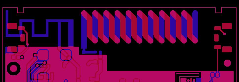
DN038 Antenna is as follows -

CC1350 STK ANTENNA is as follows -

Q2) Also in the Design Note DN038 it is mentioned that the antenna is NOT matched to 50 ohm , so I need 1pF and 12nH to make its impedance 50 ohm. For that I will have to remove ANT4 and ANT5 in the above schematic with 1pF and 12nH respectively and keep everything before them as is ? Is this correct ?

Q3) Why is the antenna slightly different (i am guessing because of the pcb thickness)? Should I implement the one in the Design Note DN038 or as in the CC ANTENNA DK/ CC1350 STK ?

In the CC-ANTENNA-DK2  Antenna Measurements Summary () Page 29, Section 2.1.6 dosen’t say anything about its actual impedance. And for matching it possibly says to use 5.6nH inductor only.

Q4) What exactly should I do for the SubGHz antenna ?

I do NOT have access to a VNA and it may not be possible for me to get access to one. So I want to make one that has the most probability of working without the need of a VNA.

  • Hi,

    Q1: Yes, you are right. But Antenna matching depends upon the PCB Layout (Gnd pattern and other components) and the casing (Plastic housing). So, it is always better to use PI network for Antenna matching on Prototypes.

    Q2: Yes, you are right. But Antenna matching depends upon the PCB Layout (Gnd pattern and other components) and the casing (Plastic housing). The same matching may not be hold good for different PCB Layout. So, it is always better to use PI network for Antenna matching on Prototypes. You can start with those components and check the RL.

    Q3: Both Antennas are same (the lengths are same - if we add each arm). In one the arm length is longer than the other but the overall length is same. You can use either of them based on your PCB Size.

    Q4: If you don't have VNA then better to copy our design exactly then you will have a better chance of getting matched.

    If you are expecting an optimum performance then better to use PI matching network and match it on Prototypes. If it is only for experimental purpose then you can start with our design values.

    Thanks,

    PM

  • Right now it's only for experimental purposes.
    So just for the sake of confirmation,
    Q1) For the 2.4GHz antenna things are exactly similar to the CC1350STK design except the ANT2 and ANT3 parts, where i can place 0 ohm for now and later when i get a VNA i can match it better by replacing them with calculated values
    OR should i actually keep everything in the CC1350 STK design including ANT2 and ANT3 and maybe change/replace them later if i get access to VNA? Which one is the best option ?
    Q2) I have already made a library part for the DN038 SubGHz antenna. So i will exactly copy the CC1350 STK matching filters etc and inplace of ANT4 and ANT5 place 1pF and 12nH ? Is this correct ?
  • Hi,

    Q1: Yes, copy everything from CC1350STK which includes AN2 & ANT3. You may need to trim ANT2 & ANT3 values on Prototypes for optimum performance.

    Q2: Yes, you can use it. Please note that you may need to trim ANT4 & ANT5 values on Prototypes for optimum performance.

    Thanks,

    PM

  • Q2: I would reuse the antenna design in the CC-Antenna-DK2 instead since the antenna design for the CC1350 SensorTag is specific for just this design.

    Regards,

        Richard

  • Richard,

    As far as i checked the antenna in CC ANTENNA DK2 and CC1350STK are similar and different from DN038. But according to the replies before, they are different because the length of the threads is different for both.

    I actually thought i would go for the antenna DN038 as it seems more general ? What are your thoughts?

  • I've implemented the DN038 antenna on a design and we got great results. Remember to keep any ground pours away from the antenna though.
  • Hello Derek,

    That is great news. Would you please mind telling me if you needed any extra passives for tuning.... basically what values of passives you used between the RF pins to the feed of antenna? Would be really helpful.

    And one more thing... when you talk about "Remember to keep any ground pours away from the antenna though." you mean to just follow the given design right? I mean in the design the ground plane starts at the base of the antenna..... no ground plane around the antenna, right?

  • On one project, we kept the same values as in the referenced design for the passives. On another project we handed it off to an RF engineer to do the match.

    On second question, you are correct - just keep the ground plane starting at the base of the antenna; no GND near the antenna.
  • Please follow DN038 as a general antenna recommendation. The antenna design on the CC1350STK is quite specific for this design due to the layout constraints.