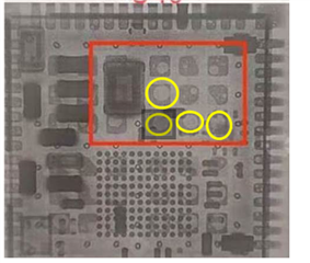
The GND pads are in the middle of this WIFI module, after actual SMT solder reflow, we find void no those GND pad.
We try to adjust reflow profile and SMT stencil design, but can't get better result.
So do those voids will affect the reliability of WIFI function?