This thread has been locked.

If you have a related question, please click the "Ask a related question" button in the top right corner. The newly created question will be automatically linked to this question.

CCS/CC3220SF-LAUNCHXL: PCB Board UART Communication - Unflash Connect issue

Part Number: CC3220SF-LAUNCHXL
Other Parts Discussed in Thread: CC3220SF, UNIFLASH, CC3200, TPS62163, TPS62162

Tool/software: Code Composer Studio

Hai, 

have a custom designed PCB based on the CC3220SF and i can not communicate uniflash and Debug 

We have not been able to flash our code even once and have not been able to connect it using uniflash to change from production to development mode. 

i followed  www.ti.com/.../swru462 (Design Checklist) ... all are fine 

share my Schematic connection 


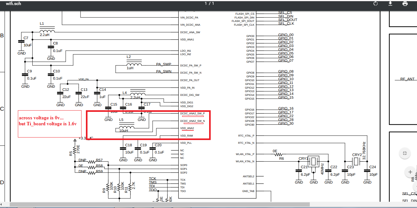
1.DCDC -ANA2-SW-P ---> 0v

2.DCDC- ANA2-SW-N ---> 0v

3.VDD- ANA2              ----> 0v

but voltage ref (1.6V)

the actual voltage is 1.6 but we are getting 0v

any other change in schematic or resistance value 

TI Schematic File Snapshot 


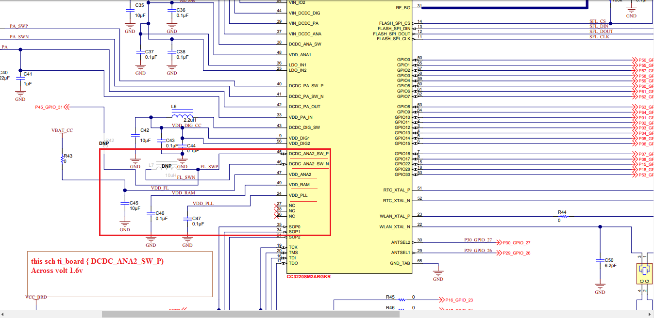
 TI_Board voltage across is fine ( 1.6V) ..

(Design Checklist)---> Followed component is use to pcb board 


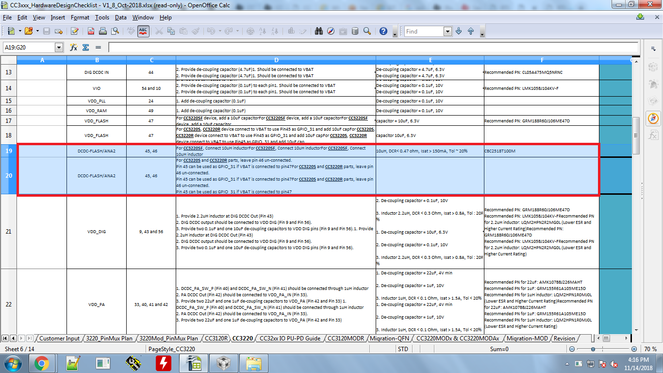
this components BOM part Number will be used ..

how to solve this issue ..?????

Following Testing voltage Mesurement

Test Point TI Board                   || My Own Board

VIN_IO1                  -> 3.3V             3.3V

VIN_IO2                  -> 3.3V              3.3V

VIN_DCDC_DIG     -> 3.3V              3.3V

VIN_DCDC_PA       -> 3.3V              3.3V

VIN_DCDC_ANA    -> 3.3V               3.3V

DCDC_ANA_SW    -> 1.9V               1.9V

VDD_ANA1             -> 1.9V              1.9V

LDO_IN1                 -> 1.9V              1.9V

LDO_IN2                 -> 1.9V              1.9V

DCDC_PA_OUT     -> 0V                  0V

VDD_PA_IN            -> 0V                  0V

DCDC_DIG_SW     -> 1.2V               1.2V

VDD_DIG1              -> 1.2V               1.2V

VDD_DIG2              -> 1.2V               1.2V

DCDC_ANA2_SW_P -> 1.6V             0V ( issue point)

DCDC_ANA2_SW_N -> 1.6V             0V ( issue point)

VDD_ANA2                -> 3.2V             0V ( issue point)

VDD_RAN                  -> 1.2V             1.2V

VDD_PLL                   -> 0V                  0V

Any other solution at this issue--> how to power up the board , uniflash also not connect..

Thanks 

SELVA

  • Hi SELVA,

    One quick comment.

    Yes, it looks that DC-DC is not functional. This issue is common in case of wrong PCB layout. Do you use 4 layers board at least? CC32xx devices are very sensitive to proper design around DC-DC.

    Jan
  • Hi Jan,

             we designed the board with 4 layer only as per the TI layout guidance.

    In case of wrong PCB layout, Please refer layout documents to function the DC-DC converter.

    otherwise I will send the gerber files, if possible send the suggestion for that. 

    Regards,

    Anandkumar T.

  • Hi Anandkumar,

    As reference you should use design files for LaunchPad and this www.ti.com/.../swru458.pdf document. But it looks that you used this documentation already. I am not aware about additional documentation. Maybe you can search at e2e forum. As I remember critical parts around DC-DC design was there discussed here some time ago. Information related to CC3200 may to be applicable to CC3220 as well.

    Please wait for additional advices from TI side.

    Jan
  • Selvaprabakaran,

    I've accepted your friend request. Please send me your design files via DM.

    BR,
    Seong
  • Hai senog,

    i'm send the message to private chat, Please check it

    Thanks

    Selva
  • Selva,

    I've reviewed your schematic and layout.

    One thing I've noted from your schematic is that there are no 100k pull ups on pin55 (UART_TX) and pin57 (UART_RX).

    From your layout:

    1) From looking at your Top Solder mask gerber file, it looks like you have GND vias placed on the ground pad of the QFN, but it is hard to determine that you have without a Drill Drawing gerber. Please confirm that you've done so exactly as shown under section 4.5 of the CC3220 Layout Guideline.

    2) The GND return for the input decoupling capacitors on pins 37, 39, and 44 are routed on the third layer, which you call Mid Layer 15. This must be routed on the second layer and must be strictly followed because it is critical for the overall performance of the device.

    3) The third layer is where the power lines to the device must be routed. It looks like Mid Layer 2 is your power plane layer.

    4) If the gerbers were simply titled incorrectly and your layers are in order, have you tried another CC3220SF IC? Were the results the same?

    5) Have you tried bypassing the TPS62163 and powering your board directly from the TPS62162 3.3-V output? Or 3.3-V power source that can provide sufficient current directly to +3.3v_IC?

    BR,

    Seong

  • Hi Seong Kim,

    Really thanks for the reply. Fault is not providing pull up resistors for TX and RX. Now its working fine.

  • Hai Seong Kim,

    Thank you very much, now issue solved , TX and RX pull up problem ...

    Regards

    SELVA