Other Parts Discussed in Thread: UNIFLASH, CC3220SF
Hi,
For some special purpose, I want to programming the CC3220SF-LAUNCHXL through the external XDS110.
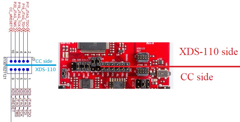
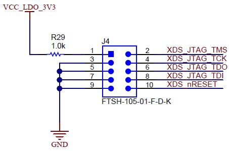
I have a LAUNCH-CC3220MODASF. and what should I do to configuring it as a independent XDS110?
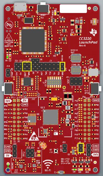
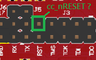
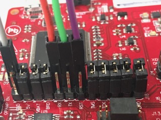
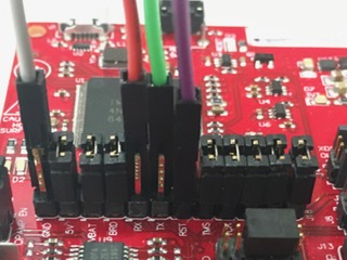
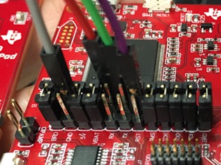
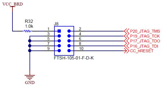
For the CC3220SF-LAUNCHXL, how should I set the related jumpers if I want to connect it with the external XDS110 (LAUNCH-CC3220MODASF)?
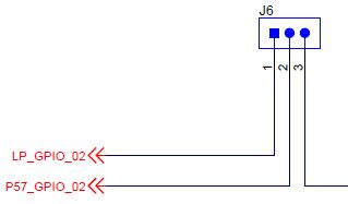
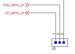
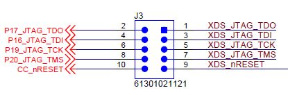
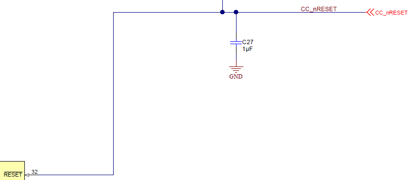
and which pins should I connect between XDS110(LAUNCH-CC3220MODASF) and CC3220SF-LAUNCHXL for UniFlash programming?
thanks a lot.
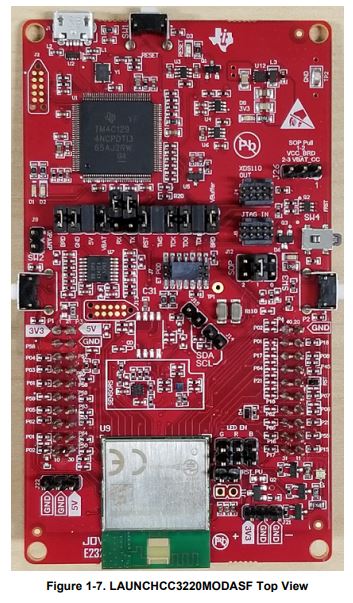
LAUNCH-CC3220MODASF
CC3220SF-LAUNCHXL