This thread has been locked.

If you have a related question, please click the "Ask a related question" button in the top right corner. The newly created question will be automatically linked to this question.

OPA547: Stability of circuit with amplifier in feedback of loop.

Part Number: OPA547
Other Parts Discussed in Thread: OPA192

Hello all, I am designing a current source and this is the design I have gone with: 
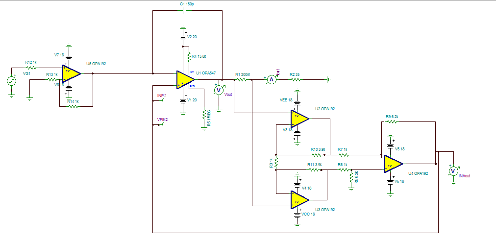
U1 is the driver with a shunt R1 in series with the output. U2, U3, U4 form an INA to convert the OPA547's output current to a voltage, and U5 is an input buffer for an ADC. The reason I inverted the INA inputs and connected the feedback to the positive terminal of the OPA547 is so that I can convert this to a voltage source by disconnecting the INA output and grounding the positive input of U1, and then adding a feedback resistor between U1's output and negative input, and then the INA output can go to an ADC to monitor current. I feel that this uses less relays. Another thing worth mentioning is that, while I understand the issues with matching in discrete INAs, I did it this way because I  needed the INA to be significantly faster than the 547, which has a GBW of 1MHz. The 192's have a GBW of 10MHz and are each in a gain less than 10, with an overall INA gain of ~55. I could not find an INA from TI with a high enough bandwidth at that gain. It may be possible that I was not using the parametric search correctly so if you could suggest a part taht would be great. 

I am aiming for +/-15V operation on the output with 300mA output capability. 

I did a few things to try to check stability and would like someone to give me some feedback to see if I did it correctly or if they have any suggestions on how to change this circuit or pick better parts, Thanks. 

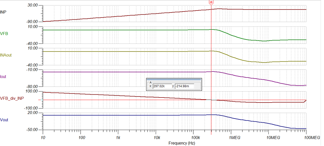
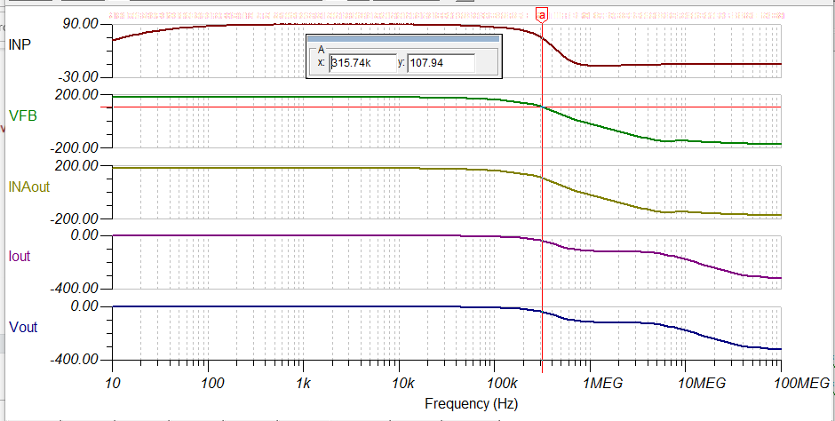
I started by grounding the VG1 input and disconnecting the feedback and adding a 0 VDC and 1VAC source and doing phase/gain AC transfer analysis in TINA. Using the post processor I plotted VFB/INP. Here is the gain plots where we can see a 0 crossing just before 300KHz. 

Then looking at the phase plot I found that VFB has a phase margin over 100 at 300Khz, which I understand means the circuit is stable. 

Finally I input a few signals and looked at DC transient settling to look at ringing. I had input steps of 100mV with .1uS rise time, a 200mV with .1uS rise time, and a 5.46V step with .1uS rise time. The last value corresponds to swinging the OPA547 from +18V 500mA to -18V -500mA. In all the cases there was no more than a 2-5% overshoot with 2 or so rings that settled within 10-20uS. That seems reasonable to me and I was mostly just hoping that the circuit eventually settles with no infinite lock up unrecoverable oscillations. 

My next step is to try to optimize C1 for whatever load capacitance I want to drive. If anyone can provide feedback on my analysis and  let me know if my assumptions are correct or if they noticed anything I should change, I would appreciate it. 

Thanks, 

Tina file attached:

stabilityanalysis.TSC

  • Not sure why you are concerned with wideband instrumentation op amp as OPA547 is only 1MHz UGBW.  Answer some of the following questions and we can propose an optimum solution.  1)  Input signal amplitude and frequency 2) Desired Iout/Vin scaling 3) All load ranges you are trying to design this for (i.e. resistive, inductive, capacitive, combinations of several? 4) Power supply voltages available?

    For background collateral see links below that will be helpful:

    www.ti.com/precisionlabs

    Look at the Stability videos

    http://e2e.ti.com/support/amplifiers/precision_amplifiers/w/design_notes/2645.solving-op-amp-stability-issues.aspx

    Download all 4 parts in PowerPoint

    You may also find attached of interest on V-I Circuit Design

    Design and Apps Current Sources_AFA.ppt

  • Thanks for the reply Tim,
    The V-I circuit design document was useful and the improved Howland pump might be the way to go instead of my design if there are any significant stability issues with it.

    1) The higher end of the input signals will be around 100KHz and the input voltages are currently around +-5V (a +-2.5V DAC going to a buffer/gain stage with gain of 2, but I can scale that up or down as needed in the buffer stage).

    2) The max desired scaling for Iout/Vin is for the +-5 Vin range to map to the full +-500mAout range of the opa547 with the .2 Ohm shunt. But again, I can scale Vin as appropriate and also switch in a different shunt with a relay to give me lower gain and that should give me better accuracy at lower Iout Ranges of the circuit. I calculated that my gain equation for Iout/Vin is 1/(R_shunt*G_INA). The INA has a gain of 55. So a .2 Ohm shunt gives an Iout/Vin of 90mA/V and will scale +-5.4Vin to +-500mAout. If I add a 5 Ohm shunt instead I can scale +-5Vin to ~+-20mAout then I will have a gain of approximately 4mA/V. So lets just say that those 2 shunt values and gains are the upper and lower extremes of what I want to use.


    3) I am trying to design for resistive and very small capacitive loads. The capacitive loads are not as important, as long as the circuit can handle just basic parasitic capacitance and smaller cap loads I will be happy .

    4) I have any arbitrary voltage up to +-24V available to me. The final output of the opa547 I was aiming for was +-15 V so the input voltages can be anything greater than that. I picked +-18V for opa192's and +-20V for opa547's in the circuit above. ( I picked a slightly higher voltage for the opa547 to have some headroom for voltage lost to the shunt drop and swing to the rails. I will still add over voltage protection to the opa192's inputs.)

    And finally, I was concerned with a wideband instrumentation amp because (from my basic understanding of stability with amplifiers in the feedback loop) I thought you wanted the feedback circuitry to be faster than the driving amp (because you could introduce significant phase shift among other things otherwise). So to be safe I wanted an INA faster than the opa547.