Other Parts Discussed in Thread: OPA551, , OPA561
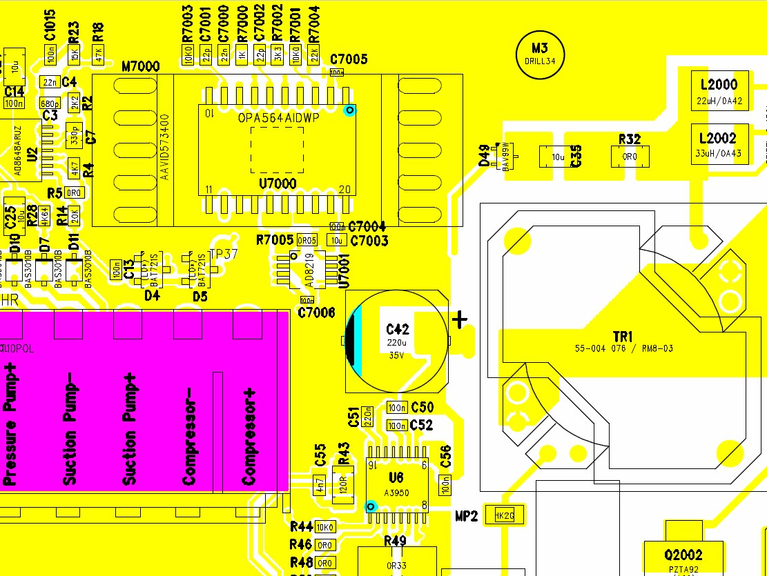
We had to replace the OPA551 with the OPA564 due to higher power demand of a newer load. Operating conditions are:
Supply is single sided @ 24 V, current drawn less than 500 mA. Input signal is sine @ 130 kHz, Vpp varies.
Transformer primary is 9 mH @ 2 Ohms.
What we observe is the following: The circuit performs well for weeks and then dies in the following sequence of events:
1) I-Flag gets stuck high, even if there is no input signal. Amp still works. (we do not monitor I-Flag)
2) I-Flag stuck high and Amp output is stuck low, < 1 V above GND.
3) Amps all of a sudden draws excessive current, frying the current shunt.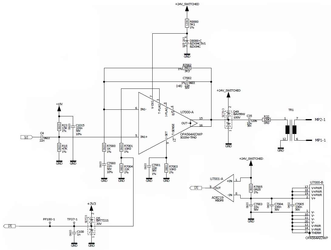
4) T-Flag never gets set high, device does not get too hot. Case @max 85 °C.
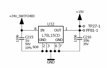
We had at first suspected the power supply sequence as possible cause for this failure and thus implemented
the very circuit from the datasheet, made up from Zener and resistor. It seemed to take longer for the Amp to fail
(weeks instead of days).
Can it be that damage is caused by firing the circuit up just once without proper power supply sequencing?
Cheers,
Andreas