Other Parts Discussed in Thread: LM1875
Basic Description:
I am having a tough problem with high frequency output oscillations with an LM675 (and also an LM1875) on 2 of the same PCBs, call them PCB1 and PCB2. The relevant schematic excerpt is attached. The normal loads connected via J20 are a 10ohm resistor in series with a 10uH-1mH linear (non-saturating) inductor. Nominal drive current range is +/- 500mA, and I need DC-10KHz output.
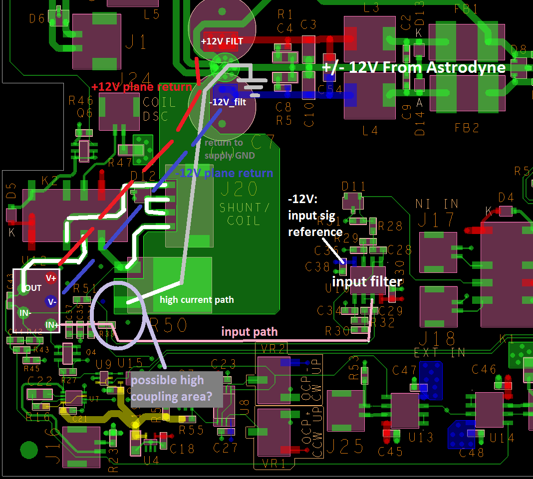
PCB Layout:
The current PCB layout is attached. I've also attached a previous PCB layout in which the problem did not occur! The differences (current vs previous) include:
- Current - 4 layers 2oz with GND, V+, V- planes, vs Previous - 2 layers 0.5oz with only GND plane
- Amplifier mounting and bypassing
- on the current, then amplifier is mounted standing up vertically into through-holes. The bypass caps are directly underneath it on the bottom side (only components on bottom side). I accidentally forgot to void the power plane connections inside the THs for the amp's power pins, so they are connected to the power planes both directly and through a via/trace on which the bypass cap sits.
- on the previous, the amplifier is laying down horizontally with pins trimmed and bent down onto SMT pads. Bypass caps sit on the same top side, with power traces hitting the bypass caps right before they reach the amp pin pads themselves
Description of problem:
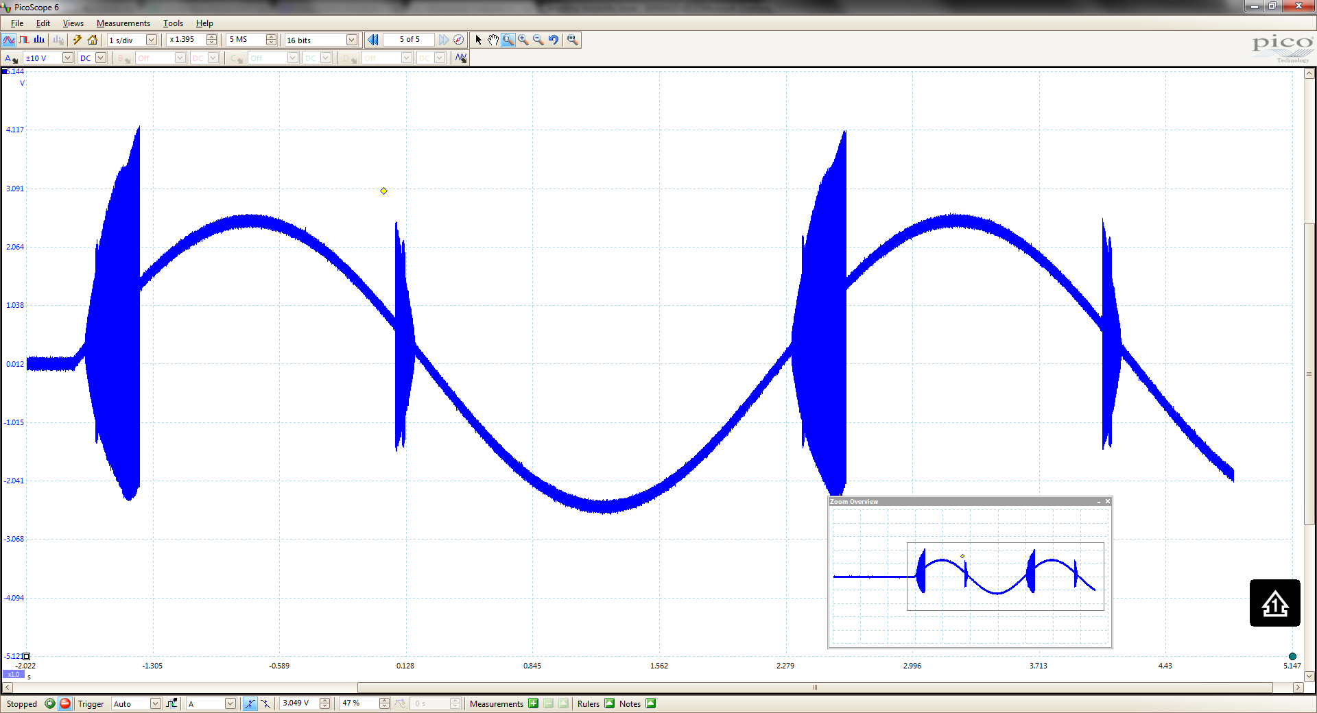
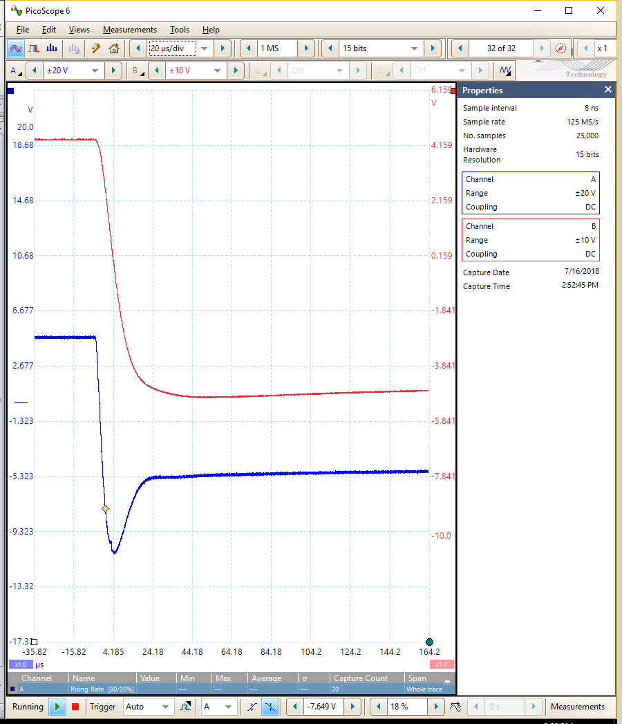
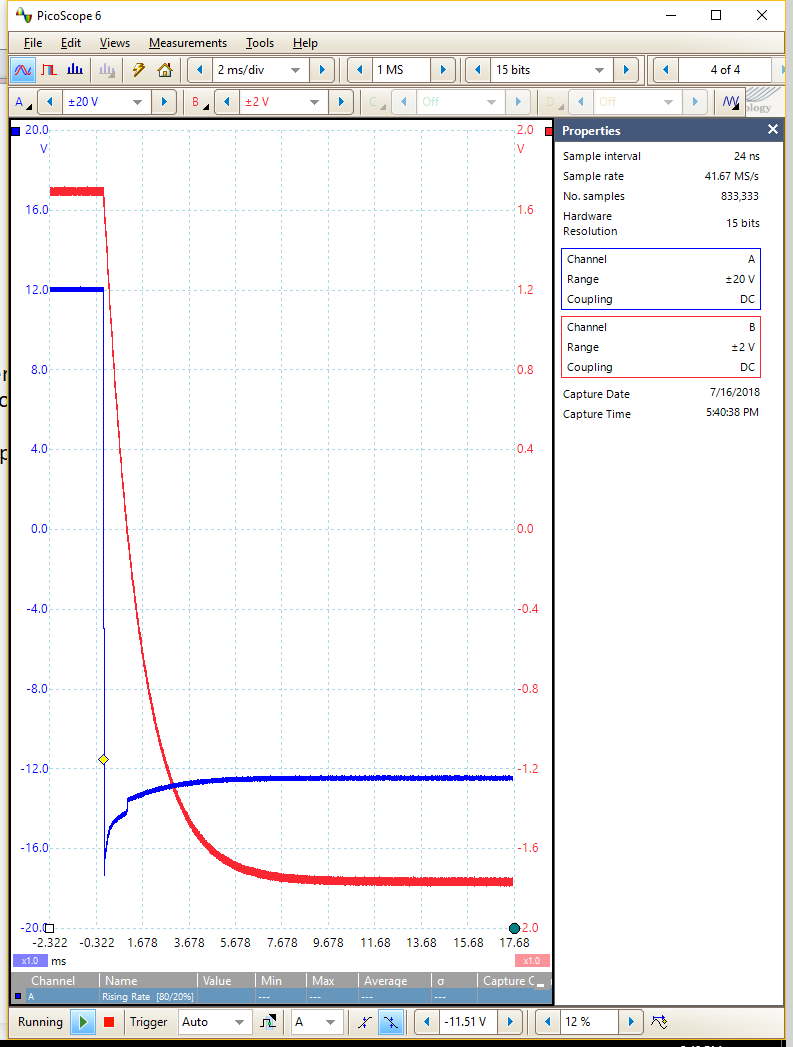
The problem I am seeing is a very high frequency (5-30MHz) large (>1Vpp often) oscillation on the amplifier output. See attached. This is at and above the amplifier GBW. This oscillation appears only at certain input voltage (and thus output current) levels, which is really really odd to me. The oscillation frequency is different depending on the I/O polarity, say typically ~25-30MHz on + side and closer to ~5MHz on the - side. It will go away if the output current magnitude is too high or too low, it has a sort of sweet spot around 50-150mA in both directions. I've messed around with the input attenuator to change the Vin / Iout relationship and it seems to follow the output current values rather than the input voltage values.
Testing performed:
I have performed the following testing on PCB #2 (the one with the LM1875 rather than the LM675) since it is not installed in it's fixture and the symptoms between the 2 were quite similar.
- Apply small capacitor (33-68pF) across J20.1-J20.2 - often greatly improves, but doesn't completely eliminate. Not totally consistent.
- Remove 6.8u tantalum bypass caps - oscillations get worse (grow in amplitude)
- install 33u ceramic caps in their place - negligible effect
- replace inductive load with short circuit (leaving resistive load in place) - negligible effect
- shorten load connection leads from ~16" to ~3" - negligible effect
- Apply 1x scope probe 3" from amplifier output - quells oscillations almost completely (acting as output to GND snubber?)
- Apply 1x scope probe directly near amplifier output - negligible effect or makes worse
- Apply discrete snubber, 22R series with 100p:
- if series inductance is within 150nH-400nH, quells oscillations (small values furnished by straight wire, wire loops, etc, very consistent results. places resonance near ~20MHz ballpark)
- if series inductance is outside this range, negligible effect
- Replace LM1875 amplifier with LM675 - quells oscillations completely
- Replace that LM675 with another LM675 - quells oscillations completely
- Move LM675 from top mounted, bottom mounted, top mounted again - oscillations always gone
Note that PCB1 exhibits the same issue as PCB2 and it is already using an LM675...
Some questions:
- Does anyone see anything criminal about my new PCB layout compared to the old one? I would really be willing to re-spin the PCB's if I had half a clue of what change I'd even make...
- Is there any reason to expect that an LM675 would behave differently than an LM1875 in this regard? I am still scratching my head at the concept that that fixed it on PCB #2, despite not obviously helping on PCB #1
- Am I just stupid for not including an amp output to ground snubber ckt? I see them on a lot of designs but I didn't include one, and it doesn't really seem like my problem is a normal load related feedback instability. The finnickyness of the snubbers in my case (150-400nH series inductance requirement) does not make me love the idea. I'd rather remove the oscillation root cause...
Attachments: