This thread has been locked.

If you have a related question, please click the "Ask a related question" button in the top right corner. The newly created question will be automatically linked to this question.

LM311: The function of two transistors at input pin of LM311

Part Number: LM311
Other Parts Discussed in Thread: TINA-TI

Dear teams,

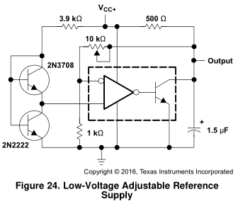
In datasheet of LM311, we provided a method to create a low-voltage adjustable reference supply from Figure 24 . But I'm not understand the necessary of these two transistors. Why not using a resistor divider to provided the input reference for LM311? Is it necessary to add a 1.5uF capacitor at output port?

Thank you for your help in advance.

Regards,

Ricardo

  • "September 1973"? I'd guess the original designer of this circuit can no longer be found next door.


    The 2N3708 is said to be a low-noise transistor.
    As far as I can see, the lower transistor is saturated, so the reference voltage is really low. I'd guess that this construction is chosen to make the input reference independent from the supply.

  • Hello Ricardo,

    It looks to be a crude low-voltage delta-Vbe reference. Basically you are seeing the difference in the Vbe's of two (different sized) transistors at the "output".

    Using two different size transistors creates slightly different Vbe voltages, but thermally the Vbe's drift will track (the difference should stay the same). A quick sim shows about 64mV at the comparator input.

    Dunno how practical the circuit is, though it is cute. It shows how to to use a comparator as a (poor) amplifier. The output transistor will be "PWM'ed" to discharge the cap (output voltage gets integrated across the 1.5uF) under negative feedback to create a "linear" output.

    There have been major breakthroughs in IC design since 1973, so there are better ways to accomplish this these days... :^)
  • Hi Paul,

    Yes, this is a well-designed circuit. I searched our power devices to find a low-voltage adjustable reference supply. But I found the lowest voltage provided by almost of reference supply devices is great than 1V. How to get a low-voltage adjustable reference supply which output lower than 1V and as accurately as possible? Do you have any idea?

    Regards,

    Ricardo

  • Hi Clemens,

    Thanks for you help. The output voltage of this circuit is very low, my purpose is to get an accurate low voltage reference supply.

    Regards,
    Ricardo
  • Hi Ricardo,

    Paul has exlained the behaviour of this circuit very well.

    If TINA-TI is working correctly then this circuit shows a temperature drift of 1.6%/°C between 27° and 60°C with the given components. But if you put two identical 2N3708 transistors into the simulation, then you will get only 0.3%/°C temperature drift. The reference voltage changes from 31.87mV to 34.82mV between 27°C and 60°C, which is a difference of about 3mV.

    Simulating two identical transistors makes sense, because at the time the datasheet was written transistor arrays like the CA3146 were widely used for these tasks. And it's imaginable that with a transistor array and an optimized collector current setting the temperature drift could even be improved. I guess that the circuit was changed some day by replacing the transistor array by two discrete transistors. But doing so will result in a desaster when using a delta-Vbe reference topology. This scheme can only work when the transistors are fabricated on the same die.

    A temperature drift of 3mV seems to be a lot. But you should not forget that the LM311 also shows an input offset voltage drift of several millivolts. So, this delta-Vbe scheme need not to be much more precise.

    And, as Clemens already mentioned the circuit is rather independent from supply voltage changes. If the 5V supply voltage increases by 5%, the reference voltage increases by only 0.3mV. This is five times less than what a simple resistive voltage divider would provide.

    Kai

  • Hi Kai,

    Thank you for your help.

    I agree with you. The discrete transistors will introduce temperature drift error. The transistors are fabricated on the same die could provide lower temperature drift error. In this way, we could get a nice reference voltage, which is a difference of about 3mV between 27° and 60°C.

    And thanks for Clemens. The lower transistor is saturated. The saturated drop voltage of lower transistor will not dramatically change when power supply ripple is not very large.

    The max input offset voltage of LM311 is about 7.5mV, unless I picked another device which shows a lower offset voltage or I couldn't get a better output supply. And the accuracy of feedback resistors will also introduce an error (If I just choose a 1% resistor). All in all, the accuracy of this reference is still better than a simple resistive voltage divider .

    Regards,

    Ricardo