This thread has been locked.

If you have a related question, please click the "Ask a related question" button in the top right corner. The newly created question will be automatically linked to this question.

TLV9004: Please check our usage.

Guru 10395 points
Part Number: TLV9004

Hi team.

Thank you for your usual support.

I want you to confirm bellow our usage.

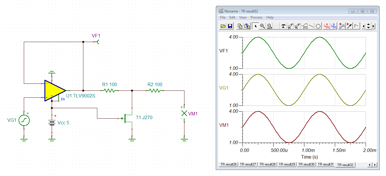
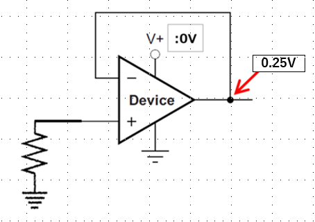
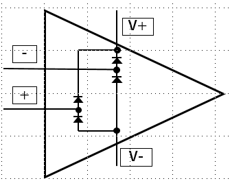
I will useTLV9004 as a voltage follower.

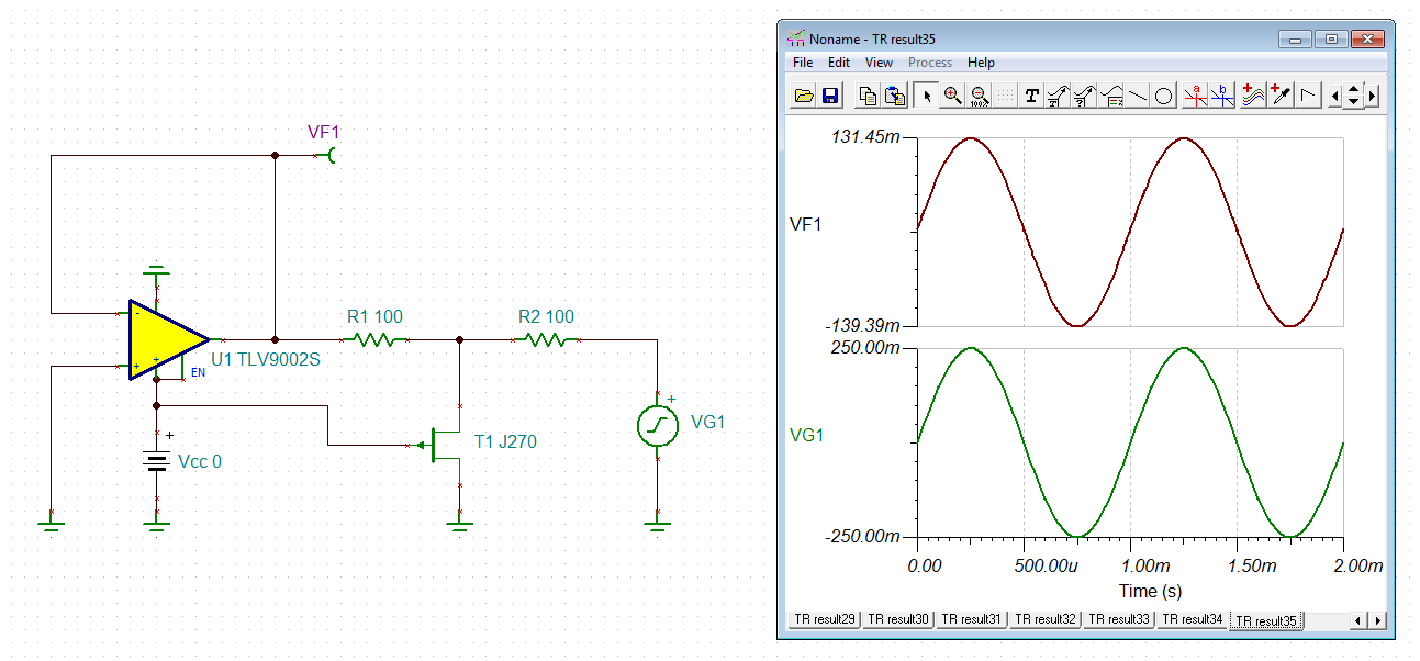
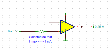
When power off , 0.25V applied to TLV9004.

Is it OK, if I use this usage?

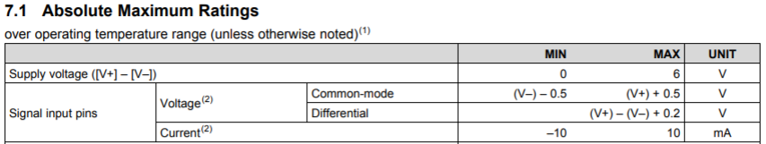
According to datasheet from 7.1, I think it is OK.


Sincerely.

Kengo.

  • Former Member
    0 Former Member
    Hello Kengo,

    I think you will be ok. Please read below for more details.

    With your device off, there will be two main concerns.

    1. Potential damage to your product due to Electrostatic Discharge (ESD). From the datasheet's maximum specifications, the absolute maximum input common-mode is 500 mV past the positive supply rail. This reflects the turn on voltage of the ESD protection diodes. So long as your are confident that you can maintain the output voltage at 0.25 V and not surpass the 0.5 V limit, you should be fine.

    2. You also need to make sure that you maintain the input current to less than 10 mA as exceeding this limit can also damage your device.

    Again, keep the voltage around 250 mV and the input current below 10 mA at all times and you should not have any problems. Hopefully this answers your question.

    Regards,
    Daniel
  • Hi Daniel.

    Thank you for your kindly answer.

    I understood your answer and additional detail.

    I have one more question.

    When I check the data sheet again, I think my usage over the maximum rating at differential.

    (0V)-(0V)+0.2V:Diffrential's maximum voltage.

    The input voltage is (+)0V and (-)0.25V in our usage.

    If it is OK, please tell me why it is OK.

    Sincerely.

    Kengo.

  • Former Member
    0 Former Member in reply to Kengo.Y
    Hello Kengo,

    If we assume that both your positive supply rail and your non-inverting input are grounded, then the set up shown will exceed the absolute maximum rating for differential input voltage.

    Could you let us know:
    1. What is driving the supply voltage at the positive rail? Is it grounded? Is it floating?
    2. What are you expecting to see at the non-inverting input?

    Then, we can give you a better idea of what to expect.

    Regards,
    Daniel
  • Hi Daniel.
    Thank you for your response.

    I understood our usage is over the absolute maximum rating for differential input voltage.

    I'll answer your questions.

    1. What is driving the supply voltage at the positive rail? Is it grounded? Is it floating?
     →It is GND(Pull down), I think.
    2. What are you expecting to see at the non-inverting input?
     →I have no idea, I have to confirm to our customer.
    Could you advice your idea in this state, if possible.

    Sincerely.
    Kengo.
  • Hi Kengo,

    eventually, this scheme could help:

    But it must be tken into consideration that JFETs can show huge production tolerances. So, this scheme might not be suited for a series production.

    What is the supply voltage of TLV2004 in operation? What is the output signal?

    Kai

  • Former Member
    0 Former Member in reply to Kengo.Y
    Hello Kengo,

    Thanks for your answers.

    It is a bit difficult to give concrete advice at this point past what we have already discussed. If we knew what the customer will be doing at the non-inverting input, that would help a lot. It would also help to know what is providing the 250 mV at the output. Finally, knowing the user application might also help.

    Kai's suggestion seems to involve a FET switch to partially isolate the op-amp's inverting input when the device is turned off. This may be an acceptable fix, depending on the system.

    Again, I will need more information regarding the input and output to be able to confidently give more information beyond what is already here.

    Regards,
    Daniel
  • Hi Daniel and Kai.

    Thank you for your reply.

    I confirmed with the customer.

    Could you check and give me your advice.

    1. What is driving the supply voltage at the positive rail? Is it grounded? Is it floating?

     →It is grounded by Pull-Down.

     2. What are you expecting to see at the non-inverting input?

        →It is 0 to 3V analog input.

    I'll wait your answer.

    Sincerely.

    Kengo.

  • Former Member
    0 Former Member in reply to Kengo.Y
    Hello Kengo,

    If the non-inverting input can be anywhere between 0 and 3 V during power off, then it is not possible to ensure that the non-inverting input will remain within 200 mV of the inverting input. This can lead to violations of the maximum differential input voltage from the datasheet and damage to the device.

    If you know the inverting input will be 250 mV in this power off stage, then you need to keep the non-inverting input as close to the inverting input as possible and always remain within the range of 50 - 450 mV. Hopefully this is possible for your customer's design.

    Let me know if you have any more questions.

    Regards,
    Daniel
  • Kengo,

    If output is within 250mV of ground with power off then no problem will occur as no significant current will flow even at higher ambient temperatures. If input signal is 3V, then a series resistor is needed to keep current low; IIN = (VIN - 0.6V) / R. This current will flow to V+ which will elevate V+ voltage by some amount. This is the main reason to keep current the current flow low.

  • Hi Daniel,Ron.
    Thank you for your support.

    Please let me check again.

    Our usage is out put is 250mV with power off when V+ is ground.
    I think our usage is over voltage about differential voltage in datasheet.
    However my understanding is our usage is no problem by your answers.
    So can you guarantee it?

    And then, can I use it up to 0.5V, if I must set current limited to 10mA or less?

    Sincerely.
    Kengo.
  • Kengo,

    10mA is the absolute maximum rated current. This AMR table comes with all the footnote warnings. So I suggest limiting current to 1mA. This current level is very low risk. However, I can't guarantee anything not specifically mentioned in the data sheet. Even in that case, I'd only point to the data sheet table.

  • Former Member
    0 Former Member in reply to Kengo.Y
    Hi Kengo,

    I have spoken with Ron about this question and am sorry if there has been confusion. According to Ron, the current specification in the datasheet assumes that the voltage specification has been violated.

    As Ron stated, if you wish to exceed the input differential voltage specification, you will need to place a resistor at the input as a precaution against an overcurrent condition.

    The absolute maximum current that is permissible is 10 mA. However, it is best to select your resistor to limit the current to a lower value, such as 1 mA, for the sake of having a safety margin.

    Again, if you exceed the maximum input differential voltage, you will need to take the precaution of placing an extra resistor in order to protect your part. Given the implementation you have described to us, you will need to take this action. Please see Ron's answer for more details.

    Hopefully this has answered your question. Let us know if you have any more doubts.

    Regards,
    Daniel
  • Hi Ron and Daniel.

    Thank you for detailed explanation.

    I understood your recommend maximum rated current.

    Please let me check again to deepen my understanding about input differential voltage.

    Bellow figure is our usage.

    My understanding is this is exceed the maximum input differential voltage.

    However, can we use it if the current is such as 1mA when the maximum input differential voltage exceed ? 

    I'm looking for ways to use our usage.

    Sincerely.

    Kengo.

  • Former Member
    0 Former Member in reply to Kengo.Y

    Hello Kengo,

    Here is a schematic describing my understanding of the part during shutdown.  The input is a 0 - 3 V signal at the non-inverting input.  The inverting input is tied to the output and held at 250 mV.  Under this scenario, the input differential voltage limitation is exceeded.  In order to protect your part from damage, you need to place a series resistor at the non-inverting input.

    This resistor needs to be selected to keep the input current to about 1 mA or less so as to avoid damaging the internal protection diodes.

    Regards,

    Daniel

  • Hi Kengo,

    this is a typical example of how difficult (or impossible) it can be to solve a problem without seeing the full schematic. To be honest, I'm totally confused by now. How can there be an input voltage of 3V when the supply voltage is down? Where does it come from? And where does the 0.25V at the output come from? And why 0.25V exactly?

    It there any chance that you can show us a detailed schematic of the circuit?

    Kai

  • Hi Daniel,Kai.

    Sorry for confusing you.

    Our usage is bellow figure.

    When it is power off, a signal input + pin is 0V fixed.

    And then 0.25V is input at outputpin.

    Is there a problem with our usage about differential voltage ?

    If there are problems, how can we use it ?

    Sincerely.

    Kengo.

  • Hi Kengo,

    in this case Ron has given the perfect answer:

    "If output is within 250mV of ground with power off then no problem will occur as no significant current will flow even at higher ambient temperatures."

    Kai
  • Hi Kai.
    Thank you for your response.

    I understood that our usage is no problem.
    But I care about exceed the maximum input differential voltage.
    Is it exceeding however not broken?

    I want to double check with you.

    Sincerely.
    Kengo.
  • Kengo,

    The input differential voltage spec isn't relevant with the power off . There are no diodes input to input. If any input current flows on the inverting input, it will flow to V+ pin if positive current (and voltage) and V- pin if negative current. No current will flow input to input.
  • Hi Kengo,

    maybe I'm wrong, but I guess the maximum differential input voltage specification "(V+) – (V–) + 0.2" is mainly relevant for supply voltages being much higher than 0V. With Vcc = 6V, e.g., the maximum differential input voltage must not exceed 6.2V, to prevent the input section from breaking down. But with Vcc = 0V such a destructive break down of input section isn't possible.

    Kai
  • Hi Ron,Kai.

    Thank you for your kind response.

    I understood very well.

    Bellow figure is my understanding. Is that correct?

    So your meaning is input(+) voltage through to V+ when it is V+ = V- = 0V.

    Because there is the diode between V+ and input(+).

    And then, we should care about input current that is 1mA or less when V+ = V- = 0V. Is it correct?

    Sincerely.

    Kengo.

  • Kengo.

    Your diode drawing is correct. The diodes can pass 1mA without issue. Any current that reaches V+ must be used (consumed) by something on the V+ bus. If the current is not consumed then V+ can rise as high as input voltage - diode voltage drop.
  • Hi Ron.
    Thank you so much for your reply.
    I understood my diode drawing is correct.
    And we'll use diodes at 1mA or less. (As your recommend)

    Sincerely.
    Kengo.