This thread has been locked.

If you have a related question, please click the "Ask a related question" button in the top right corner. The newly created question will be automatically linked to this question.

LMH6619: Voffset and Ibias according to input voltage range

Part Number: LMH6619

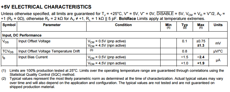
Regarding the LMH6619-

According to datasheet, the Ibais and Voffset are different in the low and high input voltage ranges. it is not written what is the input voltage value for that change.

What is the INPUT voltage limit for the low Ibias(-2.4uA/ +1.9uA) and Voffset (0.75mV/ 1.3mV) ?

How does the Ibias and Voffset change according to temperature ranges ? 

  • Hi Shirli,

    The "Conditions" column in the datasheet give the input voltage value (or VCM) and input voltage limits for the different Ibias and Voffset values; for example as shown below for the +5V supply.

    Figures 31 through 39 in the datasheet give the Voffset and Ibias variation across temperature ranges.

    Best Regards,

    Rohit

  • Hi Rohit,

    I have not understoodles yet  what is the highest input voltage that the pnp circuit is active and what is the lowest input voltage that the non circuit is active?

    If I want to compensate  the bias/offset error in all input range- it seems from dataset that there are 2 different ranges and each one of them has different Ibias/Voffset . For compensation needs, I need to know what is the input voltage that each error is active.

  • Hello Shirli,
    The transition between the npn and pnp will be gradual. In an ideal world it would be invisible to us. amplifiers designed that way are referred to as zero crossover.

    Look at Figure 33 of the datasheet. You will notice that the offset voltage is linear up to around 3.4V. below 3.4V is the PNP active region. There is then a transition region between 3.4V to 4V. The Vos is again linear above the 4V common mode. The > 4Vcm is the NPN active region. If you look at the CMRR spec on page 5, the ranges I mentioned above are also defined.