This thread has been locked.

If you have a related question, please click the "Ask a related question" button in the top right corner. The newly created question will be automatically linked to this question.

Unexpected distorsion in OPA376 and OPA2376

Other Parts Discussed in Thread: OPA340, OPA2376, OPA376, OPA316, OPA314

Dear Sir,

In some of our applications we need to generate a sinusoidal voltage signal with better than -54dB of total harmonic distorsion, i.e. less than 0.2%.
I have been using for years the OPA340 as a sallen-key to buffer and filter the source signal generated by a D/A.

The D/A is implemented as (part of) and FPGA with weighted resistors, whose generation pattern is calculated in matlab in order to minimize the second harmonic. The matlab optimization procedure takes into account equivalent impedances of the FPGA outputs as well as the external components, included the salle-key filter.

This solution works perfectly, the FPGA produces no second harmonic and the OPA340 does the same. However we recently had to design the same circuit for a 2.5V instead of 3.3V, therefore we thought that OPA340 might have been at its limits. We then changed OPA340 with OPA376 (actually OPA2376 which is double), which shall even be better than OPA340 both in distorsion, noise and offset, as I read in the datasheet.

However, the very same circuit by changing the OPA only shows a relative high distorsion!

We also verified it by temporarily changing the power supply to 3.3V also for OPA376, so that the comparison was fare.

Besides, we also discovered the by removing the feedback capacitor of the sallen-key configuration, i.e. by leaving the OPA376 and OPA340 as buffer only, the OPA376 behaviour improved a little, while the OPA340 did not change.

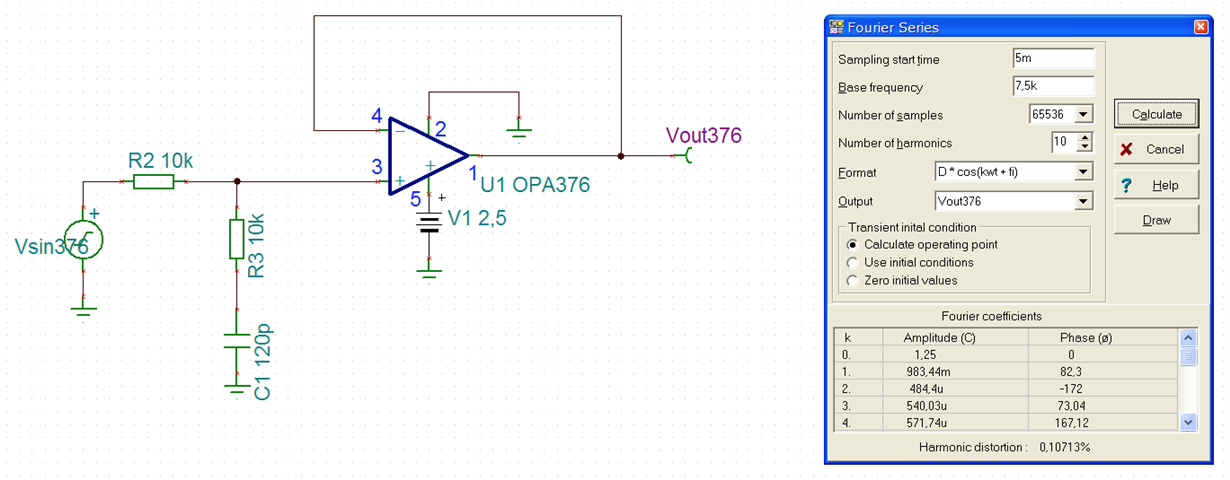
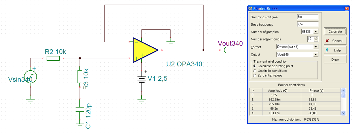
We then made some simulation, whose screenshot I am attaching below. To my surprise, even the simulation actually shows that OPA376 is introducing distorsion more than the OPA340, despite having a lower THD value in the datasheet. Of course, in both cases the actual distorsion measurements are a little worse in reality, however this is quite normal in a simulation and anyway the simulated results are worse than the datashee values.

What I kindly ask you is:

1) can you please explain me this behaviour and the eventual pitfall in the circuit ?

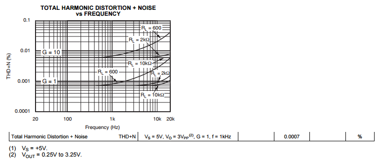
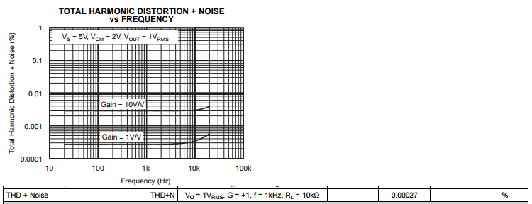
2) can you please send us the schematic of the test you perform to measure the distorsion of OPA340 (THD=0.0007%) and OPA376 (THD=0.0002%) ?

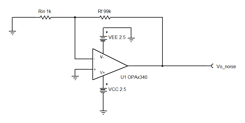
3) in that circuit we are also using OPA376 as an amplifier elsewhere, due to the stated low noise; we are however reading A/D converterd voltages with quite more noise than we expcted; could you please send also the noise test schematics?

Thank you very much for you attention and support,

Roberto Padovani

  • Roberto,

    Below please find the answer to your questions:

    1) can you please explain me this behaviour and the eventual pitfall in the circuit ?

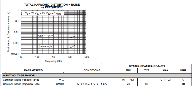
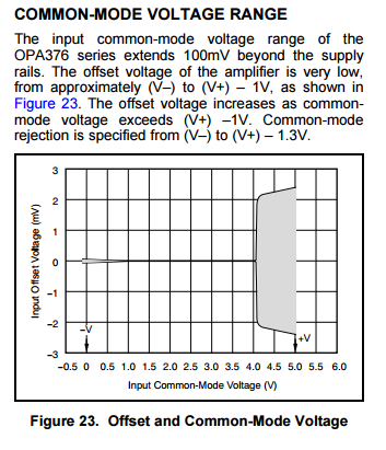
    Even though OPA376 input commn-mode voltage can operate 100mV beyond its rails, it is specified ONLY from (V-) to (V+)-1.3V (see PDS conditions column below) and thus appling rail-to-rail input signal will result in a large signal distortion caused by the non-linearity of the input stage. 

    The input common-mode voltage range issue is also shown on page 10 of datasheet - see below.

    While OPA340 CMRR also gets worse close to positive rail, its performance does not suffer as much as in the case of OPA376 - this may be seen below by looking at the OPA340 CMRR input range which is specified from (V-)-0.3V to (V+)+0.3V 

    2) can you please send us the schematic of the test you perform to measure the distorsion of OPA340 (THD=0.0007%) andOPA376 (THD=0.0002%) ?

    As may be seen on the graph below, OPA340 THD+Noise is measured for Gain +1 and +10 with the output voltage between 0.25V and 3.25V (Vout=3Vpp) on Vsupply of 5V.  

    In case of OPA376, THD+Noise is measured with Vout=1Vrms (+/-1.41Vp) and the input common-mode of 2V - therefore, the output voltage stays between 2V+/-1.41V (0.59V to 3.41V) on Vsupply of 5V.  Thus in Gain=1, the input signal does NOT get above Vcm<[(V+)-1.3V] specified in CMRR test.

    3) in that circuit we are also using OPA376 as an amplifier elsewhere, due to the stated low noise; we are however reading A/D converterd voltages with quite more noise than we expcted; could you please send also the noise test schematics?

    In order to measure an op amp noise, the circuit must be place in a large gain (+100 or +1000) to get above instrument's noise floor, with its input and output voltage at mid-supply (Vcm=0) and Vs=+/-2.5V - see below.  Operating OPA376 with the input common-mode voltage Vcm>[(V+)-1.3V] will result in much higher noise figure since the OPA376 is NOT optimized for best performance close to positive rail and for that reason is specified only for (V-)<Vcm<(V+)-1.3V - see conditions of CMRR test.

  • Marek, thank you very much for the explanation; I can of course mark the question as answered.

    However, I would like to take the chanche to ask you to suggest to me an alternative to OPA340 when the supply is only a single-ended 0V to 2.5V.
    Thank you in advance,

    Roberto
  • Roberto,

    Even though OPA340 is specified for min Vs=2.7V, it will operate down to 2.5V supply. If you need an op amp to be specified down to Vs=1.8V, please consider OPA314 or OPA316.