This thread has been locked.

If you have a related question, please click the "Ask a related question" button in the top right corner. The newly created question will be automatically linked to this question.

DP83879IVS input pins after power-up before clock

Hello,

I am using the DP83879IVS in MII mode, coupled with a Beckhoff ET1100 MAC. I notice an intermittent glitch, which happens rarely during power-up - after several tens/hundreds of power cycles: The input pins 45, 46, 48 of DP83879 (TXD0_B, TXD2_B, TXD3_B) seem to act as if they are outputting some charge / current. These pins are connected in my circuit to the ET1100 MAC, and to 2.2K pull-up / pull-down resistors. These pins are sampled by the MAC after power-up, and sometimes (rarely) the sampled values are wrong. During the sample time, the supplies are well stabilized (several tens of milliseconds after power-up), the DP83849 is held in reset since initial power-up time, and the clock input of DP83849 is stationary, no clock, pulled up by a 2.2K resistor. Probing by oscilloscope doesn't show any voltage glitch on these pins, just system noise of around 50mV peak-peak around the pull-up/down voltage of 0V or 3.3V. However, when I remove these pins (by lifting them from PCB), or when the entire DP83849 is removed, there is no more problem, even after thousands of power cycles. As soon as the DP83849 is soldered (including these pins), the problem shows after some tens/hundreds od power cycles.

What would be very useful is to have an equivalent input schematic of the on-chip circuitry inside the DP83849IVS on these 3 pins - are they just connected to a pair of CMOS gates plus a pair of reverse-biased ESD diodes? Or is there something more? I suspect that these pins may be driven during the time when there is no clock, some tens of milliseconds after power-up.

The frequency of wrong power-ups seem to depend on the slew rate of the 3.3V supply (common supply for DP83849 and ET1100 MAC) - less frequent with ~100uS risetime, more frequent with ~500uS risetime. The sampling moment is at ~80mS after 3.3V rising.

A related question: what is the input current current of the pins which have on-chip pull-up/down? For example, TXD0_B has on-chip pull-down. Datasheet shows maximum +/-10 microAmps on all inputs - this is probably wrong for the pins with on-chip pull-up/down. Also datasheet recomends external 2.2Kohm pull-up/down resistors, to counter-act the on-chip pull-up/downs. Could you be more specific about the input current that is sourced/sinked by the on-chip pull-up/downs?

Another un-related remark: datasheet SNOSAX1F revised September 2015 contains several errors related to the numbering of the timing values. The number in the AC timing requirements table does not correspond to the number in the referred picture. See for example timing T2.32.1 at page 17, which probably should correspond to T2.27.1 at page 29. Or, anotehr example, look at page 23: there are two waveforms with timings T2.14.1 and T2.14.2, one at figure 4-15 and one at figure 4-17. Most probably, the error appeared during this revision, the previous National Semiconductor datasheet of May 2008 is OK.

  • Hi,

    I am reviewing this and will provide feedback.

    Kind regards,
    Ross
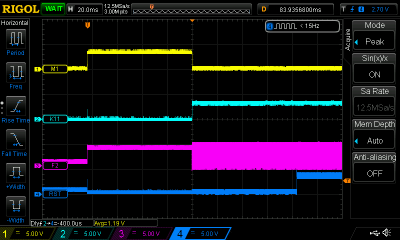
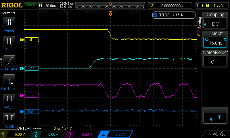
  • After thorough investigations, I have found the root problem: the DP83849IVS drives pins 45, 46, 48 (signals TXD3_B, TXD2_B, TXD0_B) immediately after power-up, until the moment when a clock pulse is applied to the X1 input (pin 70). See pictures below, same signals at two different time-scales: trace "M1" (yellow) is pin 45 of DP83849 (signal TXD3_B), trace "F2" (pink) is pin 70 (signal X1), trace "RST" (dark blue) is pin 71 (signals /RESET) - please ignore light blue trace "K11".

    Pin 45 powers up as output logic one, and falls into High impedance (input) after the first falling edge of clock - and everything happens during reset asserted. My intermittent problem was due to initial output of pin 45 - sometimes it outputs one, sometimes it outputs zero. And also the same for at least pins 46 and 48 (possibly all input pins may behave similarly).

    Can you shed some light on this weird behaviour, which strongly contradicts the dataheet? We have begun to design some counter-measures, but a deeper understanding of the chip inner working could be helpul.

  • Hi,

    There pin a CMOS level input buffers with internal resistor pull-downs and ESD structure.
    The behavior of the pins might not be known if a clock source is not present.

    I am afraid that I am not able to share any further detail on the internal circuitry of our device for competitive reasons.

    Kind regards,
    Ross
  • Hello,

    I suggest to update the datasheet with this missing information, maybe a notice like "Please notice that input pins behaviour and specifications (such as input current) are not guaranteed during the time period between power-up and the first clock pulse." The present datasheet suggests that the input pins are always inputs, no matter what, as shown in the datasheet captures below. There is no hint whatsoever that these inputs can behave as outputs during startup.

    And with this occasion maybe you can correct also the wrong figure numbering detailed previously.

    Best regards,

    A.Neacsu

  • hi Ross,

    if I well remember the process of doc update takes long time before it is implemented: do you see any chance to update the doc with a note/warning?

    for the time beeing we can just confirm that the behavior of the pins is unpredictable if no clock source is present, right?

    @ Alecsandru: is this ok for you? do you need further support on this topic?

    unfortunately, as Ross said, we can't share further details for competitive purpose...

    KR

    Vincenzo

  • @Vincenzo: The confirmation would be OK for me, I understand that datasheet update takes longer.

    @Ross, please confirm the question posted by Vincenzo: " we can just confirm that the behavior of the pins is unpredictable if no clock source is present ". That would close the topic from my point of view, that's why I proposed my previous post as a possible answer.

  • Hi,
    Correct, when a clock source is not supplied the pin behavior is unpredictable.
    Kind regards,
    Ross