This thread has been locked.

If you have a related question, please click the "Ask a related question" button in the top right corner. The newly created question will be automatically linked to this question.

DS90UB964-Q1: Line-Concatenated forward Line Length

Part Number: DS90UB964-Q1
Other Parts Discussed in Thread: ALP

Dear TI Experts,

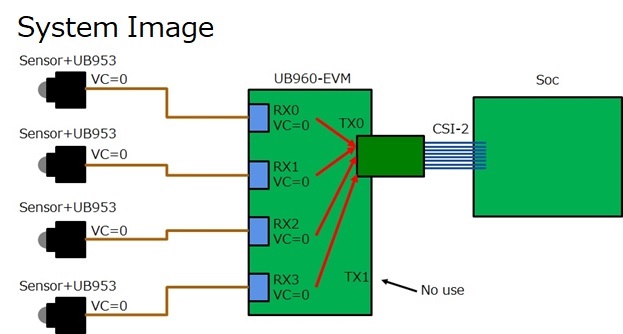
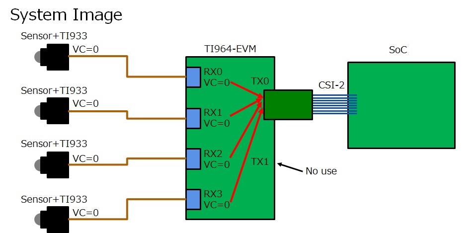
We are examining the connection 4 cameras in Line-concatenated forwarding of UB964.
(Refer System image)

There is no problem if there are 3 cameras connections,
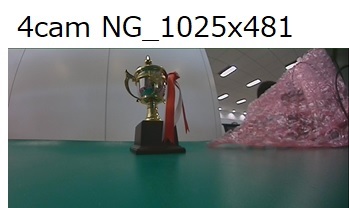
but if there are 4 cameras connections, the picture does not appear correctly.
(Refer Get image. 3cameras connections:3843x481 4cameras connections,:1025x481)

We have exceeded the Line length specification.

Please tell me the limit of Line Length at Line-concatenated forwarding.

Our environment is below.
 ・4 cameras connect (1280x480,YUV422,216Mbps/Lane)
 ・Serializer is UB933
 ・UB964 CSI output is 1600Mbps/Lane setting
 ・Output port is CSI-TX0
 ・VC:0,DT:1F 
 ・Frame Sync mode (Line-concatenated forwarding)

Thank you and best regards,

  • Hey Ken,

    I'm a little confused because your question is tagged with 964 but the block diagram says 960. Also the black diagram says 953 but the text says 933. Which devices are actually being used?

    I don't think these frame dimensions should exceed any buffer sizes. Can you read back register 0x22 while forwarding all 4 cameras to see if therew are any synchronization errors flagged?

    Best Regards,
    Casey
  • Hey Casey

    I'm sorry. It is my mistake. Block diagram was incorrect.
    The combination of UB933 and UB964 is correct.

    Register 0x22 check result is 0x01.
    synchronization error has not occurred.

    Are there any other register to check?

    Thank you and best regards,

  • Hello Ken,

    Can you please provide your programming steps used to set the 4 camera line concat mode?

    Thanks,
    Casey
  • Hey Casey

    Thank you

    We used Programing steps below.

    //e.g. $i2c, 0, 0xBD, 0x32, 1, 0x01
    $i2c:I2c command(unique)
    0:I2c address length
    0xBD:I2c Device address
    0x32::I2c Register address
    1:I2c Data length
    0x01:Data value

    ===============================================================================

    /////////////////////////////////////////////////////////////////
    // For UB933/UB964(EVM)@4ch
    //  DES_Write_Add:BD (8bit:7A_7bit:3D)
    //  SER_Write_Add:ch1-91,ch2-92,ch3-93,ch4-94
    //                             (8bit:22,24,26,28_7bit:11,12,13,14)
    /////////////////////////////////////////////////////////////////

    //PORT&ID setting////////////////////////////
    $i2c, 0, 0xBD, 0x32, 1, 0x01 //CSI_PORT_SEL [0]TX_WRITE_PORT_0 [0]0:disable/1:enable

    //RX0
    $i2c, 0, 0xBD, 0x4C, 1, 0x01 //FPD3_PORT_SEL [5:4]RX_READ_PORT 00:PORT0/01:PORT1/10:PORT2/11:PORT3
                                                  //  [0]RX_WRITE_PORT_0 0:disable/1:enable
    $i2c, 0, 0xBD, 0x5C, 1, 0x22 //SER_ALIAS_ID [7:1]SER_ALIAS_ID
    $i2c, 0, 0xBD, 0x5D, 1, 0x34 //Slave_ID[0] [7:1]Slave_ID0
    $i2c, 0, 0xBD, 0x65, 1, 0x34 //SlaveAlias[0] [7:1]Slave_ALIAS_ID0
    $i2c, 0, 0xBD, 0x70, 1, 0x1F //RAW10_ID [7:6]VC [5:0]DT

    //RX1
    $i2c, 0, 0xBD, 0x4C, 1, 0x12 //FPD3_PORT_SEL [5:4]RX_READ_PORT 00:PORT0/01:PORT1/10:PORT2/11:PORT3
                                                   //  [1]RX_WRITE_PORT_1 0:disable/1:enable
    $i2c, 0, 0xBD, 0x5C, 1, 0x24 //SER_ALIAS_ID [7:1]SER_ALIAS_ID
    $i2c, 0, 0xBD, 0x5D, 1, 0x34 //Slave_ID[0] [7:1]Slave_ID0
    $i2c, 0, 0xBD, 0x65, 1, 0x34 //SlaveAlias[0] [7:1]Slave_ALIAS_ID0
    $i2c, 0, 0xBD, 0x70, 1, 0x1F //RAW10_ID [7:6]VC [5:0]DT

    //RX2
    $i2c, 0, 0xBD, 0x4C, 1, 0x24 //FPD3_PORT_SEL [5:4]RX_READ_PORT 00:PORT0/01:PORT1/10:PORT2/11:PORT3
                                                  //  [1]RX_WRITE_PORT_1 0:disable/1:enable
    $i2c, 0, 0xBD, 0x5C, 1, 0x26 //SER_ALIAS_ID [7:1]SER_ALIAS_ID
    $i2c, 0, 0xBD, 0x5D, 1, 0x34 //Slave_ID[0] [7:1]Slave_ID0
    $i2c, 0, 0xBD, 0x65, 1, 0x34 //SlaveAlias[0] [7:1]Slave_ALIAS_ID0
    $i2c, 0, 0xBD, 0x70, 1, 0x1F //RAW10_ID [7:6]VC [5:0]DT

    //RX3
    $i2c, 0, 0xBD, 0x4C, 1, 0x38 //FPD3_PORT_SEL [5:4]RX_READ_PORT 00:PORT0/01:PORT1/10:PORT2/11:PORT3
                                                   //  [1]RX_WRITE_PORT_1 0:disable/1:enable
    $i2c, 0, 0xBD, 0x5C, 1, 0x28 //SER_ALIAS_ID [7:1]SER_ALIAS_ID
    $i2c, 0, 0xBD, 0x5D, 1, 0x34 //Slave_ID[0] [7:1]Slave_ID0
    $i2c, 0, 0xBD, 0x65, 1, 0x34 //SlaveAlias[0] [7:1]Slave_ALIAS_ID0
    $i2c, 0, 0xBD, 0x70, 1, 0x1F //RAW10_ID [7:6]VC [5:0]DT

    //GPIO setting////////////////////////////
    $i2c, 0, 0xBD, 0x4C, 1, 0x0F //FPD3_PORT_SEL [5:4]RX_READ_PORT 00:PORT0/01:PORT1/10:PORT2/11:PORT3
                                                  //  [0]RX_WRITE_PORT_0 0:disable/1:enable
    $i2c, 0, 0xBD, 0x58, 1, 0x58 //BCC_CONFIG [6]I2C_PASS_THROUGH 0:disable/1:enable
    //RX0
    $i2c, 0, 0x91, 0x01, 1, 0x20 //Control reg VDDIO=1.8V
    $i2c, 0, 0x91, 0x0D, 1, 0x59 //[6]GPO1_remoteEN 0:disable/1:enable[Fsync]
                                                 //[4]GPO1_EN 0:disable/1:enable[Fsync]
                                                 //[3]GPO0_OUTPUT_Value[XCLR]
                                                 //[0]GPO0_EN[XCLR]
    $wait,500

    //RX1
    $i2c, 0, 0x92, 0x01, 1, 0x20 //Control reg VDDIO=1.8V
    $i2c, 0, 0x92, 0x0D, 1, 0x59 //[6]GPO1_remoteEN 0:disable/1:enable[Fsync]
                                                  //[4]GPO1_EN 0:disable/1:enable[Fsync]
                                                  //[3]GPO0_OUTPUT_Value[XCLR]
                                                  //[0]GPO0_EN[XCLR]
    $wait,500

    //RX2
    $i2c, 0, 0x93, 0x01, 1, 0x20 //Control reg VDDIO=1.8V
    $i2c, 0, 0x93, 0x0D, 1, 0x59 //[6]GPO1_remoteEN 0:disable/1:enable[Fsync]
                                                  //[4]GPO1_EN 0:disable/1:enable[Fsync]
                                                  //[3]GPO0_OUTPUT_Value[XCLR]
                                                  //[0]GPO0_EN[XCLR]
    $wait,500

    //RX3
    $i2c, 0, 0x94, 0x01, 1, 0x20 //Control reg VDDIO=1.8V
    $i2c, 0, 0x94, 0x0D, 1, 0x59 //[6]GPO1_remoteEN 0:disable/1:enable[Fsync]
                                                  //[4]GPO1_EN 0:disable/1:enable[Fsync]
                                                  //[3]GPO0_OUTPUT_Value[XCLR]
                                                  //[0]GPO0_EN[XCLR]
    $wait,500

    //FS setting////////////////////////////
    $i2c, 0, 0xBD, 0x6E, 1, 0xA8 //BC_GPIO_CTL0 [7:4]BC_GPIO1_SEL 1010:FrameSync Signal
    $i2c, 0, 0xBD, 0x18, 1, 0x01 //FS_CTL [7:4]FS_MODE 0000:Internal Generated FS USE PORT0
                                                  //  [0]FS_GEN_Enable 0:disable/1:enable
    $i2c, 0, 0xBD, 0x12, 1, 0x91 //GPIO2_PIN_CTL [7:5]GPIO2_OUT_SEL 100:Framesync signal
                                                  //  [4:2]GPIO2_OUT_SRC 100:Device Status
                                                  //  [0]GPIO2_OUT_EN 0:disable/1:enable

    $i2c, 0, 0xBD, 0x19, 1, 0x02 //FS_HIGH_TIME_1 60fps
    $i2c, 0, 0xBD, 0x1A, 1, 0xB3 //FS_HIGH_TIME_0 60fps
    $i2c, 0, 0xBD, 0x1B, 1, 0x02 //FS_LOW_TIME_1 60fps
    $i2c, 0, 0xBD, 0x1C, 1, 0xB3 //FS_LOW_TIME_0 60fps

    //CSI output setting////////////////////////////
    $i2c, 0, 0xBD, 0x7C, 1, 0xC0 //PORT_CONFIG2 [7:6] Raw10 8-bit mode
                                                   //00:Normal_Raw10_Mpde/10:8-bit_using_upper/11:8-bit_using_lower
    $i2c, 0, 0xBD, 0x1F, 1, 0x00 //CSI_PLL_CTL [1:0]00:1.5/1.6Gbps_10:800Mbps/11:400Mbps
    $i2c, 0, 0xBD, 0xBC, 1, 0x25 //FV_MINI_TIME
    $i2c, 0, 0xBD, 0x20, 1, 0x00 //FWD_CTL1 [7]FWD_PORT3 0:enable/1:disable
                                                  //         [6]FWD_PORT2 0:enable/1:disable
                                                  //         [5]FWD_PORT1 0:enable/1:disable
                                                  //         [4]FWD_PORT0 0:enable/1:disable
    $i2c, 0, 0xBD, 0x21, 1, 0x0C //FWD_CTL2 [3:2]CSI0_SYCN_FWD
                                                   //00:disable/01:BasicSync/10:Interleave/11:Concatenated

    $i2c, 0, 0xBD, 0x33, 1, 0x03 //CSI_CTL [5:4]CSI_lane 00:4lanes/01:3lanes/10:2lanes/11:1lane
                                                  //   [1]Continuous_clock_mode 0:disable/1:enable
                                                  //   [0]CSI_output 0:disable/1:enable

    ================================================================================

    Thank you and best regards,

  • Hello,

    I will need a couple days to review this. I will plan to respond back on next Tuesday

    Best Regards,
    Casey
  • Hey Casey

    I'm Sorry,during the confirmation of the program.

    Is it possible to tell me the horizontal size limit in Line-concatenated forwarding mode?

    We want it as information at the time of other verification cases.

    Thank you and best regards,

  • Hi Ken,

    Are you able to send all four video streams using round robin forwarding?

    Best,

    Jiashow

  • Hi Ken,

    I would like to get some more information. Are you using YUV422 10 bit or 8 bit? Can you let me know what you read on reg 0x22?

    Best,

    Jiashow

  • Hey Jiashow

    1,Are you able to send all four video streams using round robin forwarding?
     ⇒Yes I am. I got image 1280x1920 in size(1920=480x4cam) that like Interleave or BasicSynchronize.

    2,I would like to get some more information. Are you using YUV422 10 bit or 8 bit?
     ⇒YUV422 8bit.

    3,Can you let me know what you read on reg 0x22?
     ⇒Reg 0x22 is 0x01.
      synchronization error has not occurred.

    best regards

  • Hi Ken,

    There's definitely a limit when using line concatenate mode, I'm working on verifying the limit. In the meantime, could you let me know if you are seeing any CSI errors? Such as buffer error in DES reg 0x4E[4] and CSI errors in DES reg 0x7A and 0x7B?

    Best,

    Jiashow

  • Hi Jiashow

    Thank you working on verifying the limit.

    The confirmation result of Des reg is below.(CSI-2 output is 1600Mbps/Lane)
    DES reg 0x4E : 0x55 (<=First Read, 0x04<=Second Read)
     [bit7]:1: Change of line length detected
     [bit4] 1: Packet Buffer error detected
     [bit2] 1: Frequency measurement stable
     [bit0] 1: Change of line count detected

    DES reg 0x7A : 0x00
    DES reg 0x7B : 0x00

    If a buffer error occurs, does 0x4E[bit4] continue to be 1 even if cleared on read?
    Even after the second read, 0x4E[bit4] remains 0.
    Is it safe to assume that no buffer errors have been detected in this case?

    Best Regards

  • Thanks Ken! Please give me a couple more days to look into this. But to answer your question, if after the second read, the buffer error continues to show 0, that means there's no buffer errors detected since the last read.

    In the meantime, it would be great if you could provide the register dump between the 3 camera case and the 4 camera case and highlight the differences between the two. I would like to see if there's any differences between the two cases.

    Best,

    Jiashow

  • Hi Jiashow

    How about verifying the limit.
    Do you run into difficulties.

    Best Regards

  • Hi Ken,

    Could you provide the register dump between the 3 camera case and the 4 camera case and highlight the differences between the two? I would like to see if there's any differences between the two cases.

    Best,

    Jiashow

  • Hi Jiashow      
          
    I'm sorry.      
    I forgot to provide register settings for the 3 camera case.
    Provides each register setting.
          
    ・ 3camera case      
    /////////////////////////////////////////////////////////////////      
    // For UB933/UB964(EVM)@3ch      
    // DES Config      
    // DES_Write_Add:BD (8bit:7A_7bit:3D)      
    // SER_Write_Add:ch1-91,ch2-92,ch3-93,ch4-94      
    //                            (8bit:22,24,26,28_7bit:11,12,13,14)      
    /////////////////////////////////////////////////////////////////      
          
    //PORT&ID setting////////////////////////////      
    $i2c, 0, 0xBD, 0x32, 1, 0x01 //CSI_PORT_SEL [0]TX_WRITE_PORT_0 [0]0:disable/1:enable     
          
    //RX0      
    $i2c, 0, 0xBD, 0x4C, 1, 0x01 //FPD3_PORT_SEL [5:4]RX_READ_PORT 00:PORT0/01:PORT1/10:PORT2/11:PORT3     
                                                   //  [0]RX_WRITE_PORT_0 0:disable/1:enable
    $i2c, 0, 0xBD, 0x5C, 1, 0x22 //SER_ALIAS_ID [7:1]SER_ALIAS_ID    
    $i2c, 0, 0xBD, 0x5D, 1, 0x34 //Slave_ID[0] [7:1]Slave_ID0    
    $i2c, 0, 0xBD, 0x65, 1, 0x34 //SlaveAlias[0] [7:1]Slave_ALIAS_ID0     
    $i2c, 0, 0xBD, 0x70, 1, 0x1F //RAW10_ID [7:6]VC [5:0]DT    
          
    //RX1      
    $i2c, 0, 0xBD, 0x4C, 1, 0x12 //FPD3_PORT_SEL [5:4]RX_READ_PORT 00:PORT0/01:PORT1/10:PORT2/11:PORT3     
                                                   //  [1]RX_WRITE_PORT_1 0:disable/1:enable
    $i2c, 0, 0xBD, 0x5C, 1, 0x24 //SER_ALIAS_ID [7:1]SER_ALIAS_ID    
    $i2c, 0, 0xBD, 0x5D, 1, 0x34 //Slave_ID[0] [7:1]Slave_ID0    
    $i2c, 0, 0xBD, 0x65, 1, 0x34 //SlaveAlias[0] [7:1]Slave_ALIAS_ID0     
    $i2c, 0, 0xBD, 0x70, 1, 0x1F //RAW10_ID [7:6]VC [5:0]DT    
          
    //RX2      
    $i2c, 0, 0xBD, 0x4C, 1, 0x24 //FPD3_PORT_SEL [5:4]RX_READ_PORT 00:PORT0/01:PORT1/10:PORT2/11:PORT3     
                                                   //  [2]RX_WRITE_PORT_2 0:disable/1:enable
    $i2c, 0, 0xBD, 0x5C, 1, 0x26 //SER_ALIAS_ID [7:1]SER_ALIAS_ID    
    $i2c, 0, 0xBD, 0x5D, 1, 0x34 //Slave_ID[0] [7:1]Slave_ID0    
    $i2c, 0, 0xBD, 0x65, 1, 0x34 //SlaveAlias[0] [7:1]Slave_ALIAS_ID0     
    $i2c, 0, 0xBD, 0x70, 1, 0x1F //RAW10_ID [7:6]VC [5:0]DT    
          
    //GPIO setting////////////////////////////      
    $i2c, 0, 0xBD, 0x4C, 1, 0x07 //FPD3_PORT_SEL [5:4]RX_READ_PORT 00:PORT0/01:PORT1/10:PORT2/11:PORT3     
                                                   //  [0]RX_WRITE_PORT_0 0:disable/1:enable
    $i2c, 0, 0xBD, 0x58, 1, 0x58 //BCC_CONFIG [6]I2C_PASS_THROUGH 0:disable/1:enable     
    //RX0      
    $i2c, 0, 0x91, 0x01, 1, 0x20 //Control reg VDDIO=1.8V     
    $i2c, 0, 0x91, 0x0D, 1, 0x59 //[6]GPO1_remoteEN 0:disable/1:enable[Fsync]     
                                                 //[4]GPO1_EN 0:disable/1:enable[Fsync]  
                                                 //[3]GPO0_OUTPUT_Value[XCLR]  
                                                 //[0]GPO0_EN[XCLR]  
    $wait,500      
          
    //RX1      
    $i2c, 0, 0x92, 0x01, 1, 0x20 //Control reg VDDIO=1.8V     
    $i2c, 0, 0x92, 0x0D, 1, 0x59 //[6]GPO1_remoteEN 0:disable/1:enable[Fsync]     
                                                 //[4]GPO1_EN 0:disable/1:enable[Fsync]  
                                                 //[3]GPO0_OUTPUT_Value[XCLR]  
                                                 //[0]GPO0_EN[XCLR]  
    $wait,500      
          
    //RX2      
    $i2c, 0, 0x93, 0x01, 1, 0x20 //Control reg VDDIO=1.8V     
    $i2c, 0, 0x93, 0x0D, 1, 0x59 //[6]GPO1_remoteEN 0:disable/1:enable[Fsync]     
                                                 //[4]GPO1_EN 0:disable/1:enable[Fsync]  
                                                 //[3]GPO0_OUTPUT_Value[XCLR]  
                                                 //[0]GPO0_EN[XCLR]  
    $wait,500      
          
    //FS setting////////////////////////////      
    $i2c, 0, 0xBD, 0x6E, 1, 0xA8 //BC_GPIO_CTL0 [7:4]BC_GPIO1_SEL 1010:FrameSync Signal      
    $i2c, 0, 0xBD, 0x18, 1, 0x01 //FS_CTL [7:4]FS_MODE 0000:Internal Generated FS USE PORT0     
                                                  //  [0]FS_GEN_Enable 0:disable/1:enable 
    $i2c, 0, 0xBD, 0x12, 1, 0x91 //GPIO2_PIN_CTL [7:5]GPIO2_OUT_SEL 100:Framesync signal     
                                                 //  [4:2]GPIO2_OUT_SRC 100:Device Status
                                                 //  [0]GPIO2_OUT_EN 0:disable/1:enable
          
    $i2c, 0, 0xBD, 0x19, 1, 0x02 //FS_HIGH_TIME_1     
    $i2c, 0, 0xBD, 0x1A, 1, 0xB3 //FS_HIGH_TIME_0     
    $i2c, 0, 0xBD, 0x1B, 1, 0x02 //FS_LOW_TIME_1     
    $i2c, 0, 0xBD, 0x1C, 1, 0xB3 //FS_LOW_TIME_0     
          
    //CSI output setting////////////////////////////      
    $i2c, 0, 0xBD, 0x7C, 1, 0xC0 //PORT_CONFIG2 [7:6] Raw10 8-bit mode     
                                                   //00:Normal_Raw10_Mpde/10:8-bit_using_upper/11:8-bit_using_lower  
    $i2c, 0, 0xBD, 0x1F, 1, 0x00 //CSI_PLL_CTL [1:0]00:1.5/1.6Gbps_10:800Mbps/11:400Mbps     
    $i2c, 0, 0xBD, 0xBC, 1, 0x25 //FV_MINI_TIME     
    $i2c, 0, 0xBD, 0x20, 1, 0x80 //FWD_CTL1 [7]FWD_PORT3 0:enable/1:disable     
                                                  //         [6]FWD_PORT2 0:enable/1:disable  
                                                  //         [5]FWD_PORT1 0:enable/1:disable  
                                                  //         [4]FWD_PORT0 0:enable/1:disable  
    $i2c, 0, 0xBD, 0x21, 1, 0x0C //FWD_CTL2 [3:2]CSI0_SYCN_FWD     
                                                  //00:disable/01:BasicSync/10:Interleave/11:Concatenated   
          
    $i2c, 0, 0xBD, 0x33, 1, 0x03 //CSI_CTL [5:4]CSI_lane 00:4lanes/01:3lanes/10:2lanes/11:1lane     
                                                  //   [1]Continuous_clock_mode 0:disable/1:enable 
                                                  //   [0]CSI_output 0:disable/1:enable 

           
    Line ・ 4camera case      
    1 /////////////////////////////////////////////////////////////////      
    2 // For UB933/UB964(EVM)@4ch      
    3 // DES Config      
    4 // DES_Write_Add:BD (8bit:7A_7bit:3D)      
    5 // SER_Write_Add:ch1-91,ch2-92,ch3-93,ch4-94      
    6 //                            (8bit:22,24,26,28_7bit:11,12,13,14)      
    7 /////////////////////////////////////////////////////////////////      
    8       
    9 //PORT&ID setting////////////////////////////      
    10 $i2c, 0, 0xBD, 0x32, 1, 0x01 //CSI_PORT_SEL [0]TX_WRITE_PORT_0 [0]0:disable/1:enable     
    11       
    12 //RX0      
    13 $i2c, 0, 0xBD, 0x4C, 1, 0x01 //FPD3_PORT_SEL [5:4]RX_READ_PORT 00:PORT0/01:PORT1/10:PORT2/11:PORT3     
    14                                                //  [0]RX_WRITE_PORT_0 0:disable/1:enable
    15 $i2c, 0, 0xBD, 0x5C, 1, 0x22 //SER_ALIAS_ID [7:1]SER_ALIAS_ID    
    16 $i2c, 0, 0xBD, 0x5D, 1, 0x34 //Slave_ID[0] [7:1]Slave_ID0    
    17 $i2c, 0, 0xBD, 0x65, 1, 0x34 //SlaveAlias[0] [7:1]Slave_ALIAS_ID0     
    18 $i2c, 0, 0xBD, 0x70, 1, 0x1F //RAW10_ID [7:6]VC [5:0]DT    
    19       
    20 //RX1      
    21 $i2c, 0, 0xBD, 0x4C, 1, 0x12 //FPD3_PORT_SEL [5:4]RX_READ_PORT 00:PORT0/01:PORT1/10:PORT2/11:PORT3     
    22                                                //  [1]RX_WRITE_PORT_1 0:disable/1:enable
    23 $i2c, 0, 0xBD, 0x5C, 1, 0x24 //SER_ALIAS_ID [7:1]SER_ALIAS_ID    
    24 $i2c, 0, 0xBD, 0x5D, 1, 0x34 //Slave_ID[0] [7:1]Slave_ID0    
    25 $i2c, 0, 0xBD, 0x65, 1, 0x34 //SlaveAlias[0] [7:1]Slave_ALIAS_ID0     
    26 $i2c, 0, 0xBD, 0x70, 1, 0x1F //RAW10_ID [7:6]VC [5:0]DT    
    27       
    28 //RX2      
    29 $i2c, 0, 0xBD, 0x4C, 1, 0x24 //FPD3_PORT_SEL [5:4]RX_READ_PORT 00:PORT0/01:PORT1/10:PORT2/11:PORT3     
    30                                                //  [2]RX_WRITE_PORT_2 0:disable/1:enable
    31 $i2c, 0, 0xBD, 0x5C, 1, 0x26 //SER_ALIAS_ID [7:1]SER_ALIAS_ID    
    32 $i2c, 0, 0xBD, 0x5D, 1, 0x34 //Slave_ID[0] [7:1]Slave_ID0    
    33 $i2c, 0, 0xBD, 0x65, 1, 0x34 //SlaveAlias[0] [7:1]Slave_ALIAS_ID0     
    34 $i2c, 0, 0xBD, 0x70, 1, 0x1F //RAW10_ID [7:6]VC [5:0]DT    
    35       
    36 //RX3      
    37 $i2c, 0, 0xBD, 0x4C, 1, 0x38 //FPD3_PORT_SEL [5:4]RX_READ_PORT 00:PORT0/01:PORT1/10:PORT2/11:PORT3     
    38                                                //  [3]RX_WRITE_PORT_3 0:disable/1:enable
    39 $i2c, 0, 0xBD, 0x5C, 1, 0x28 //SER_ALIAS_ID [7:1]SER_ALIAS_ID    
    40 $i2c, 0, 0xBD, 0x5D, 1, 0x34 //Slave_ID[0] [7:1]Slave_ID0    
    41 $i2c, 0, 0xBD, 0x65, 1, 0x34 //SlaveAlias[0] [7:1]Slave_ALIAS_ID0     
    42 $i2c, 0, 0xBD, 0x70, 1, 0x1F //RAW10_ID [7:6]VC [5:0]DT    
    43       
    44 //GPIO setting////////////////////////////      
    45 $i2c, 0, 0xBD, 0x4C, 1, 0x0F //FPD3_PORT_SEL [5:4]RX_READ_PORT 00:PORT0/01:PORT1/10:PORT2/11:PORT3     
    46                                                //  [0]RX_WRITE_PORT_0 0:disable/1:enable
    47 $i2c, 0, 0xBD, 0x58, 1, 0x58 //BCC_CONFIG [6]I2C_PASS_THROUGH 0:disable/1:enable     
    48 //RX0      
    49 $i2c, 0, 0x91, 0x01, 1, 0x20 //Control reg VDDIO=1.8V     
    50 $i2c, 0, 0x91, 0x0D, 1, 0x59 //[6]GPO1_remoteEN 0:disable/1:enable[Fsync]     
    51                                               //[4]GPO1_EN 0:disable/1:enable[Fsync]  
    52                                               //[3]GPO0_OUTPUT_Value[XCLR]  
    53                                               //[0]GPO0_EN[XCLR]  
    54 $wait,500      
    55       
    56 //RX1      
    57 $i2c, 0, 0x92, 0x01, 1, 0x20 //Control reg VDDIO=1.8V     
    58 $i2c, 0, 0x92, 0x0D, 1, 0x59 //[6]GPO1_remoteEN 0:disable/1:enable[Fsync]     
    59                                               //[4]GPO1_EN 0:disable/1:enable[Fsync]  
    60                                               //[3]GPO0_OUTPUT_Value[XCLR]  
    61                                               //[0]GPO0_EN[XCLR]  
    62 $wait,500      
    63       
    64 //RX2      
    65 $i2c, 0, 0x93, 0x01, 1, 0x20 //Control reg VDDIO=1.8V     
    66 $i2c, 0, 0x93, 0x0D, 1, 0x59 //[6]GPO1_remoteEN 0:disable/1:enable[Fsync]     
    67                                               //[4]GPO1_EN 0:disable/1:enable[Fsync]  
    68                                               //[3]GPO0_OUTPUT_Value[XCLR]  
    69                                               //[0]GPO0_EN[XCLR]  
    70 $wait,500      
    71       
    72 //RX3      
    73 $i2c, 0, 0x94, 0x01, 1, 0x20 //Control reg VDDIO=1.8V     
    74 $i2c, 0, 0x94, 0x0D, 1, 0x59 //[6]GPO1_remoteEN 0:disable/1:enable[Fsync]     
    75                                               //[4]GPO1_EN 0:disable/1:enable[Fsync]  
    76                                               //[3]GPO0_OUTPUT_Value[XCLR]  
    77                                               //[0]GPO0_EN[XCLR]  
    78 $wait,500      
    79       
    80 //FS setting////////////////////////////      
    81 $i2c, 0, 0xBD, 0x6E, 1, 0xA8 //BC_GPIO_CTL0 [7:4]BC_GPIO1_SEL 1010:FrameSync Signal      
    82 $i2c, 0, 0xBD, 0x18, 1, 0x01 //FS_CTL [7:4]FS_MODE 0000:Internal Generated FS USE PORT0     
    83                                               //  [0]FS_GEN_Enable 0:disable/1:enable 
    84 $i2c, 0, 0xBD, 0x12, 1, 0x91 //GPIO2_PIN_CTL [7:5]GPIO2_OUT_SEL 100:Framesync signal     
    85                                               //  [4:2]GPIO2_OUT_SRC 100:Device Status
    86                                               //  [0]GPIO2_OUT_EN 0:disable/1:enable
    87       
    88 $i2c, 0, 0xBD, 0x19, 1, 0x02 //FS_HIGH_TIME_1     
    89 $i2c, 0, 0xBD, 0x1A, 1, 0xB3 //FS_HIGH_TIME_0     
    90 $i2c, 0, 0xBD, 0x1B, 1, 0x02 //FS_LOW_TIME_1     
    91 $i2c, 0, 0xBD, 0x1C, 1, 0xB3 //FS_LOW_TIME_0     
    92       
    93 //CSI output setting////////////////////////////      
    94 $i2c, 0, 0xBD, 0x7C, 1, 0xC0 //PORT_CONFIG2 [7:6] Raw10 8-bit mode     
    95                                                //00:Normal_Raw10_Mpde/10:8-bit_using_upper/11:8-bit_using_lower  
    96 $i2c, 0, 0xBD, 0x1F, 1, 0x00 //CSI_PLL_CTL [1:0]00:1.5/1.6Gbps_10:800Mbps/11:400Mbps     
    97 $i2c, 0, 0xBD, 0xBC, 1, 0x25 //FV_MINI_TIME     
    98 $i2c, 0, 0xBD, 0x20, 1, 0x00 //FWD_CTL1 [7]FWD_PORT3 0:enable/1:disable     
    99                                               //         [6]FWD_PORT2 0:enable/1:disable  
    100                                             //         [5]FWD_PORT1 0:enable/1:disable  
    101                                             //         [4]FWD_PORT0 0:enable/1:disable  
    102 $i2c, 0, 0xBD, 0x21, 1, 0x0C //FWD_CTL2 [3:2]CSI0_SYCN_FWD     
    103                                               //00:disable/01:BasicSync/10:Interleave/11:Concatenated   
    104       
    105 $i2c, 0, 0xBD, 0x33, 1, 0x03 //CSI_CTL [5:4]CSI_lane 00:4lanes/01:3lanes/10:2lanes/11:1lane     
    106                                               //   [1]Continuous_clock_mode 0:disable/1:enable 
    107                                               //   [0]CSI_output 0:disable/1:enable 
           
    Differences between the two is below.      
    (Changes from 3 camera cases to 4 camera cases.)   
     ・RX port3 Enable setting add      
      0x4C:0x38 Line37
      0x5C:0x28 Line39
      0x5D:0x34 Line40
      0x65:0x34 Line41
      0x70:0x1F Line42
           
     ・Write Enable for RX port 0~2 => 0~3
      0x4C:0x07=>0x0F Line45
           
     ・RX port3 Serializer-GPIOsetting add
      0x01:0x20 Line73
      0x0D:0x59 Line74
           
     ・Forword Enale RX port 0~2 => 0~3
      0x20:0x80=>0x00 Line94
           
    Best Regards      

  • Hi Ken,

    Could you provide a register dump? I'd like to compare the register differences between the two config.

    Best,

    Jiashow

  • Hi Jiashow,

    Please check the register dump.

    [REGISTERS]
    Device = ALP Nano 1 - DS90UB964, Connector 1
    Comments = "UB964-3cam"
    Reg = 0,0x0000,0x7A
    Reg = 0,0x0001,0x00
    Reg = 0,0x0002,0x1E
    Reg = 0,0x0003,0x30
    Reg = 0,0x0004,0xC2
    Reg = 0,0x0005,0x01
    Reg = 0,0x0006,0x00
    Reg = 0,0x0007,0xFE
    Reg = 0,0x0008,0x1C
    Reg = 0,0x0009,0x10
    Reg = 0,0x000A,0x79
    Reg = 0,0x000B,0x79
    Reg = 0,0x000C,0x0F
    Reg = 0,0x000D,0x09
    Reg = 0,0x000E,0x04
    Reg = 0,0x000F,0xFF
    Reg = 0,0x0010,0x00
    Reg = 0,0x0011,0x00
    Reg = 0,0x0012,0x91
    Reg = 0,0x0013,0x00
    Reg = 0,0x0014,0x00
    Reg = 0,0x0015,0x00
    Reg = 0,0x0016,0x00
    Reg = 0,0x0017,0x00
    Reg = 0,0x0018,0x01
    Reg = 0,0x0019,0x02
    Reg = 0,0x001A,0xB3
    Reg = 0,0x001B,0x02
    Reg = 0,0x001C,0xB3
    Reg = 0,0x001D,0x00
    Reg = 0,0x001E,0x04
    Reg = 0,0x001F,0x00
    Reg = 0,0x0020,0x80
    Reg = 0,0x0021,0x0C
    Reg = 0,0x0022,0x01
    Reg = 0,0x0023,0x00
    Reg = 0,0x0024,0x00
    Reg = 0,0x0025,0x00
    Reg = 0,0x0026,0x00
    Reg = 0,0x0027,0x00
    Reg = 0,0x0028,0x00
    Reg = 0,0x0029,0x00
    Reg = 0,0x002A,0x00
    Reg = 0,0x002B,0x00
    Reg = 0,0x002C,0x00
    Reg = 0,0x002D,0x00
    Reg = 0,0x002E,0x00
    Reg = 0,0x002F,0x00
    Reg = 0,0x0030,0x00
    Reg = 0,0x0031,0x00
    Reg = 0,0x0032,0x00
    Reg = 0,0x0033,0x03
    Reg = 0,0x0034,0x00
    Reg = 0,0x0035,0x03
    Reg = 0,0x0036,0x00
    Reg = 0,0x0037,0x05
    Reg = 0,0x0038,0x00
    Reg = 0,0x0039,0x00
    Reg = 0,0x003A,0x00
    Reg = 0,0x0040,0x00
    Reg = 0,0x0041,0xA3
    Reg = 0,0x0042,0x01
    Reg = 0,0x0043,0x01
    Reg = 0,0x004C,0x00
    Reg = 0,0x004D,0x03
    Reg = 0,0x004E,0x04
    Reg = 0,0x004F,0x2F
    Reg = 0,0x0050,0x40
    Reg = 0,0x0051,0x00
    Reg = 0,0x0052,0x00
    Reg = 0,0x0053,0x00
    Reg = 0,0x0054,0x00
    Reg = 0,0x0055,0x00
    Reg = 0,0x0056,0x00
    Reg = 0,0x0057,0x00
    Reg = 0,0x0058,0x58
    Reg = 0,0x0059,0x00
    Reg = 0,0x005A,0x00
    Reg = 0,0x005B,0xB0
    Reg = 0,0x005C,0x22
    Reg = 0,0x005D,0x34
    Reg = 0,0x005E,0x00
    Reg = 0,0x005F,0x00
    Reg = 0,0x0060,0x00
    Reg = 0,0x0061,0x00
    Reg = 0,0x0062,0x00
    Reg = 0,0x0063,0x00
    Reg = 0,0x0064,0x00
    Reg = 0,0x0065,0x34
    Reg = 0,0x0066,0x00
    Reg = 0,0x0067,0x00
    Reg = 0,0x0068,0x00
    Reg = 0,0x0069,0x00
    Reg = 0,0x006A,0x00
    Reg = 0,0x006B,0x00
    Reg = 0,0x006C,0x00
    Reg = 0,0x006D,0x7F
    Reg = 0,0x006E,0xA8
    Reg = 0,0x006F,0x88
    Reg = 0,0x0070,0x1F
    Reg = 0,0x0071,0x2C
    Reg = 0,0x0072,0xE4
    Reg = 0,0x0073,0x01
    Reg = 0,0x0074,0xE1
    Reg = 0,0x0075,0x0A
    Reg = 0,0x0076,0x00
    Reg = 0,0x0077,0xC5
    Reg = 0,0x0078,0x00
    Reg = 0,0x0079,0x01
    Reg = 0,0x007A,0x00
    Reg = 0,0x007B,0x00
    Reg = 0,0x007C,0xC3
    Reg = 0,0x007D,0x00
    Reg = 0,0x007E,0x00
    Reg = 0,0x00B0,0x10
    Reg = 0,0x00B1,0x14
    Reg = 0,0x00B2,0x1F
    Reg = 0,0x00B3,0x08
    Reg = 0,0x00B4,0x25
    Reg = 0,0x00B5,0x00
    Reg = 0,0x00B6,0x18
    Reg = 0,0x00B7,0x00
    Reg = 0,0x00B8,0xFF
    Reg = 0,0x00B9,0x03
    Reg = 0,0x00BA,0x03
    Reg = 0,0x00BB,0x74
    Reg = 0,0x00BC,0x25
    Reg = 0,0x00BD,0x00
    Reg = 0,0x00BE,0x00
    Reg = 0,0x00D0,0x00
    Reg = 0,0x00D1,0x43
    Reg = 0,0x00D2,0x84
    Reg = 0,0x00D3,0x17
    Reg = 0,0x00D4,0x60
    Reg = 0,0x00D5,0xF8
    Reg = 0,0x00D6,0x07
    Reg = 0,0x00D7,0x00
    Reg = 0,0x00D8,0x00
    Reg = 0,0x00D9,0x00
    Reg = 0,0x00DA,0x00
    Reg = 0,0x00DB,0x00
    Reg = 0,0x00F0,0x5F
    Reg = 0,0x00F1,0x55
    Reg = 0,0x00F2,0x42
    Reg = 0,0x00F3,0x39
    Reg = 0,0x00F4,0x36
    Reg = 0,0x00F5,0x34
    Reg = 0,0x00F8,0x00
    Reg = 0,0x00F9,0x00
    Reg = 0,0x00FA,0x00
    Reg = 0,0x00FB,0x00

    [REGISTERS]
    Device = ALP Nano 1 - DS90UB964, Connector 1
    Comments = "UB964-4cam"
    Reg = 0,0x0000,0x7A
    Reg = 0,0x0001,0x00
    Reg = 0,0x0002,0x1E
    Reg = 0,0x0003,0x30
    Reg = 0,0x0004,0xC2
    Reg = 0,0x0005,0x01
    Reg = 0,0x0006,0x00
    Reg = 0,0x0007,0xFE
    Reg = 0,0x0008,0x1C
    Reg = 0,0x0009,0x10
    Reg = 0,0x000A,0x79
    Reg = 0,0x000B,0x79
    Reg = 0,0x000C,0x0F
    Reg = 0,0x000D,0x09
    Reg = 0,0x000E,0x04
    Reg = 0,0x000F,0xFF
    Reg = 0,0x0010,0x00
    Reg = 0,0x0011,0x00
    Reg = 0,0x0012,0x91
    Reg = 0,0x0013,0x00
    Reg = 0,0x0014,0x00
    Reg = 0,0x0015,0x00
    Reg = 0,0x0016,0x00
    Reg = 0,0x0017,0x00
    Reg = 0,0x0018,0x01
    Reg = 0,0x0019,0x02
    Reg = 0,0x001A,0xB3
    Reg = 0,0x001B,0x02
    Reg = 0,0x001C,0xB3
    Reg = 0,0x001D,0x00
    Reg = 0,0x001E,0x04
    Reg = 0,0x001F,0x00
    Reg = 0,0x0020,0x00
    Reg = 0,0x0021,0x0C
    Reg = 0,0x0022,0x01
    Reg = 0,0x0023,0x00
    Reg = 0,0x0024,0x00
    Reg = 0,0x0025,0x00
    Reg = 0,0x0026,0x00
    Reg = 0,0x0027,0x00
    Reg = 0,0x0028,0x00
    Reg = 0,0x0029,0x00
    Reg = 0,0x002A,0x00
    Reg = 0,0x002B,0x00
    Reg = 0,0x002C,0x00
    Reg = 0,0x002D,0x00
    Reg = 0,0x002E,0x00
    Reg = 0,0x002F,0x00
    Reg = 0,0x0030,0x00
    Reg = 0,0x0031,0x00
    Reg = 0,0x0032,0x00
    Reg = 0,0x0033,0x03
    Reg = 0,0x0034,0x00
    Reg = 0,0x0035,0x03
    Reg = 0,0x0036,0x00
    Reg = 0,0x0037,0x05
    Reg = 0,0x0038,0x00
    Reg = 0,0x0039,0x00
    Reg = 0,0x003A,0x00
    Reg = 0,0x0040,0x00
    Reg = 0,0x0041,0xA3
    Reg = 0,0x0042,0x01
    Reg = 0,0x0043,0x01
    Reg = 0,0x004C,0x00
    Reg = 0,0x004D,0x03
    Reg = 0,0x004E,0x04
    Reg = 0,0x004F,0x2F
    Reg = 0,0x0050,0x40
    Reg = 0,0x0051,0x00
    Reg = 0,0x0052,0x00
    Reg = 0,0x0053,0x00
    Reg = 0,0x0054,0x00
    Reg = 0,0x0055,0x00
    Reg = 0,0x0056,0x00
    Reg = 0,0x0057,0x00
    Reg = 0,0x0058,0x58
    Reg = 0,0x0059,0x00
    Reg = 0,0x005A,0x00
    Reg = 0,0x005B,0xB0
    Reg = 0,0x005C,0x22
    Reg = 0,0x005D,0x34
    Reg = 0,0x005E,0x00
    Reg = 0,0x005F,0x00
    Reg = 0,0x0060,0x00
    Reg = 0,0x0061,0x00
    Reg = 0,0x0062,0x00
    Reg = 0,0x0063,0x00
    Reg = 0,0x0064,0x00
    Reg = 0,0x0065,0x34
    Reg = 0,0x0066,0x00
    Reg = 0,0x0067,0x00
    Reg = 0,0x0068,0x00
    Reg = 0,0x0069,0x00
    Reg = 0,0x006A,0x00
    Reg = 0,0x006B,0x00
    Reg = 0,0x006C,0x00
    Reg = 0,0x006D,0x7F
    Reg = 0,0x006E,0xA8
    Reg = 0,0x006F,0x88
    Reg = 0,0x0070,0x1F
    Reg = 0,0x0071,0x2C
    Reg = 0,0x0072,0xE4
    Reg = 0,0x0073,0x01
    Reg = 0,0x0074,0xE1
    Reg = 0,0x0075,0x0A
    Reg = 0,0x0076,0x00
    Reg = 0,0x0077,0xC5
    Reg = 0,0x0078,0x00
    Reg = 0,0x0079,0x01
    Reg = 0,0x007A,0x00
    Reg = 0,0x007B,0x00
    Reg = 0,0x007C,0xC3
    Reg = 0,0x007D,0x00
    Reg = 0,0x007E,0x00
    Reg = 0,0x00B0,0x10
    Reg = 0,0x00B1,0x14
    Reg = 0,0x00B2,0x1F
    Reg = 0,0x00B3,0x08
    Reg = 0,0x00B4,0x25
    Reg = 0,0x00B5,0x00
    Reg = 0,0x00B6,0x18
    Reg = 0,0x00B7,0x00
    Reg = 0,0x00B8,0xFF
    Reg = 0,0x00B9,0x03
    Reg = 0,0x00BA,0x03
    Reg = 0,0x00BB,0x74
    Reg = 0,0x00BC,0x25
    Reg = 0,0x00BD,0x00
    Reg = 0,0x00BE,0x00
    Reg = 0,0x00D0,0x00
    Reg = 0,0x00D1,0x43
    Reg = 0,0x00D2,0x84
    Reg = 0,0x00D3,0x17
    Reg = 0,0x00D4,0x60
    Reg = 0,0x00D5,0xF8
    Reg = 0,0x00D6,0x07
    Reg = 0,0x00D7,0x00
    Reg = 0,0x00D8,0x00
    Reg = 0,0x00D9,0x00
    Reg = 0,0x00DA,0x00
    Reg = 0,0x00DB,0x00
    Reg = 0,0x00F0,0x5F
    Reg = 0,0x00F1,0x55
    Reg = 0,0x00F2,0x42
    Reg = 0,0x00F3,0x39
    Reg = 0,0x00F4,0x36
    Reg = 0,0x00F5,0x34
    Reg = 0,0x00F8,0x00
    Reg = 0,0x00F9,0x00
    Reg = 0,0x00FA,0x00
    Reg = 0,0x00FB,0x00

    Best Regards  

  • Hi Jiashow,

    >There's definitely a limit when using line concatenate mode, I'm working on verifying the limit.

      Sorry,How these status Now.

    Best Regards

  • Hi Ken,

    From the register dump you provided, the only register difference is 0x20. Let me follow up with my team to see what this means.

    Best,

    Jiashow

  • Hi Ken,

    Actually I realized reg 0x20 is the port forwarding register. There seems to be no difference in the setting between the two cases then. Let me follow up with my team to see if we can get more insights into this.

    Best,

    Jiashow

  • Hi Ken,

    One thing I would like to ask: Could you double check to make sure your processor is able to receive the horizontal data/resolution in the 4 cam usecase?

    Best,

    Jiashow

  • Hi Jiashow

    Thank you for your reply and follow up.

    >Could you double check to make sure your processor is able to receive the horizontal data/resolution in the 4 cam usecase?
    We are investigating it.
    Also, We are Checking MIPI Waveform.

    Please give me a couple more days.

    Best Regards

    Ken

  • Thanks Ken.

    Based on my discussion with our design team, we believe our 964 should be able to output all four imagers in line concatenation mode, so please let us know if your processor is able to handle this.

    Best,

    Jiashow

  • Hi Jiashow

    Result of confirming the MIPI waveform,UB964 output was no problem.
    Reason is below.
    Word count of ShortPacket is Expected value and PacketData of LongPacket is Expected value.

    Processer teams say that may not able to output all four imagers in line concatenation mode.
    I will consider again that the environment for processor.

    Thank you for long support.

    Best Regards,

    Ken

  • Thanks for the update, Ken!