This thread has been locked.

If you have a related question, please click the "Ask a related question" button in the top right corner. The newly created question will be automatically linked to this question.

TLK10232: Channel switch function doesn't work well

Part Number: TLK10232

Hi Team,

I posted thread 5 month ago, and got an answer as below but it doesn't work in my customer's board. May I double check if these commands are really enough for channel switching using MDIO?

Could you send me a EVM macro to connect ChA HS to ChB LS in 9 hours? I have a EVM now so I can check it tomorrow morning.

I have to have a meeting with the customer to clarify this issue tomorrow afternoon (I might need to highly escalate this if we will be not able to solve this issue within this weekend)

//Setting for DATA Switch TX (LSB=>HSA direction)
To Ch-A phy address; 
Write 1'b0 to 0x1E.0017 bit 12 (DST_PIN_SW_EN)
Write 2’b10 to 0x1E.0018 bits 15:14 (DST_DATA_SRC_SEL[1:0]) //Selects data from Low Speed CHB to High Speed CHA

//Setting for DATA Switch RX (HS=>LS direction)
To Ch-A Ch-B phy address; 
Write 1'b0 to 0x1E.0019 bit 12 (DSR_PIN_SW_EN)
Write 2’b11 to 0x1E.001A bits 15:14 (DSR_DATA_SRC_SEL[1:0])

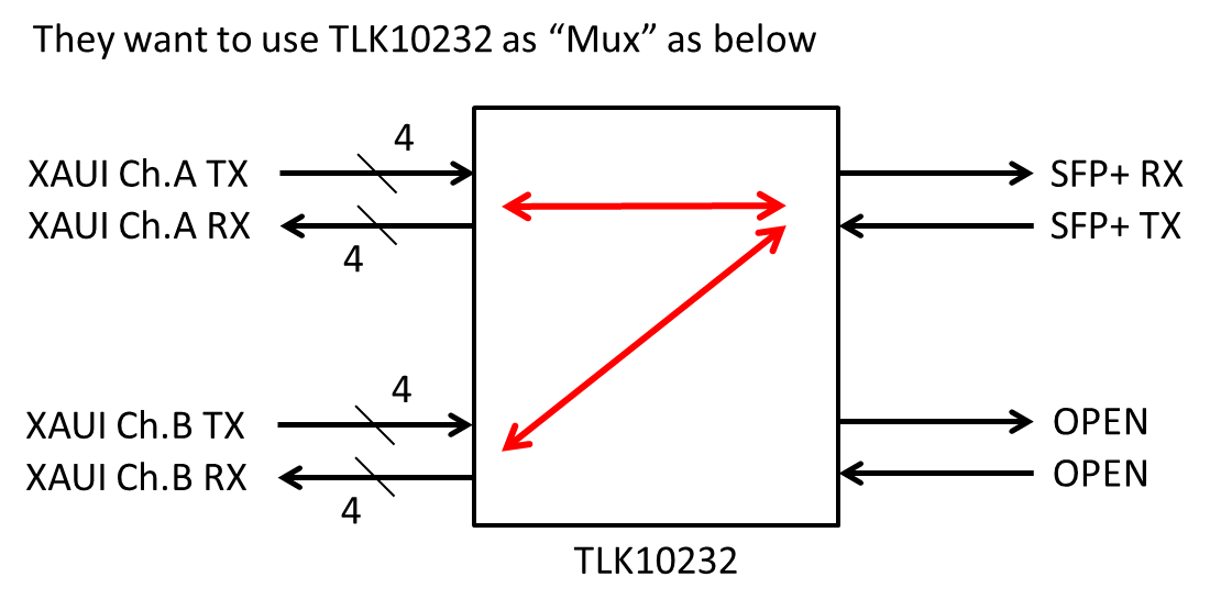
My customer would like to switch LSs to chA HS as below. And they will use 10G-KR mode. They plan to connect SFP+ module at ChA HS so they send the commend below prior to the command for switching above.

PA:0b00000 DA:0b11110(0x1E) REG_AD:0x0000 WR_DATA:0x8610
PA:0b00000 DA:0b11110(0x1E) REG_AD:0x001D WR_DATA:0x0000
PA:0b00000 DA:0b00111(0x07) REG_AD:0x0000 WR_DATA:0x2000
PA:0b00000 DA:0b00001(0x01) REG_AD:0x0096 WR_DATA:0x0000
PA:0b00000 DA:0b11110(0x1E) REG_AD:0x8020 WR_DATA:0x03FF
PA:0b00000 DA:0b11110(0x1E) REG_AD:0x0004 WR_DATA:0xD500
PA:0b00000 DA:0b11110(0x1E) REG_AD:0x000E WR_DATA:0x0008

PA:0b00001 DA:0b11110(0x1E) REG_AD:0x001D WR_DATA:0x0000
PA:0b00001 DA:0b00111(0x07) REG_AD:0x0000 WR_DATA:0x2000
PA:0b00001 DA:0b00001(0x01) REG_AD:0x0096 WR_DATA:0x0000
PA:0b00001 DA:0b11110(0x1E) REG_AD:0x8020 WR_DATA:0x03FF
PA:0b00001 DA:0b11110(0x1E) REG_AD:0x0004 WR_DATA:0xD500
PA:0b00001 DA:0b11110(0x1E) REG_AD:0x000E WR_DATA:0x0008

After sending these commands, they could not read DATA_SWITCH_STATUS register(The read values are always 0x0000).

Regards,

Takashi Onawa

  • Hi Takashi,

    According their application, customer is interfacing with SFP+ optical modules, hence, they need to adjust some parameters to optimize the link between the TLK and the optical module for the transmit path (Channel A). So, first of all they should to verify the path LSA ==> HSA,

    PA:0b00000 DA:0b11110(0x1E) REG_AD:0x0000 WR_DATA:0x8610 // Reset
    PA:0b00000 DA:0b11110(0x1E) REG_AD:0x001D WR_DATA:0x0000 // Clock Selection
    PA:0b00000 DA:0b00111(0x07) REG_AD:0x0000 WR_DATA:0x2000 // Disable Auto-negotiation
    PA:0b00000 DA:0b00001(0x01) REG_AD:0x0096 WR_DATA:0x0000 // Disable Link Training
    PA:0b00000 DA:0b11110(0x1E) REG_AD:0x8020 WR_DATA:0x03FF //Adjust parameters manually instead link training

    PA:0b00000 DA:0b11110(0x1E) REG_AD:0x0003 WR_DATA:0xA848// HS_SERDES_CONTROL_2 Default Values
    PA:0b00000 DA:0b11110(0x1E) REG_AD:0x0004 WR_DATA:0xD500 // HS_SERDES_CONTROL_3 Default Values


    *** Since device is interfacing with optical modules, parameters such as HS_SWING, HS_ENTRACK, HS_EQPRE, HS_CDRFMULT, HS_CDRTHR, HS_PEAK_DISABLE should be changed according every system (AC losses, length of traces, cables, etc.) to optimize the link.***


    PA:0b00000 DA:0b11110(0x1E) REG_AD:0x000E WR_DATA:0x0008 //Data-path reset once the desired configuration is set

    At this point the device is configured, so, user needs to try different settings for HS_SERDES_CONTROL_2 & 3 to avoid BER. Please monitor errors through HS_ERROR_COUNTER.
    Once the best settings for HS_SERDES_CONTROL_2&3 are got it, configure the switch data source:

    //Setting for DATA Switch TX (LSB=>HSA direction) CONFIGURE CHANNEL A
    //To Ch-A phy address;
    Write 1'b0 to 0x1E.0017 bit 12 (DST_PIN_SW_EN)
    Write 2’b10 to 0x1E.0018 bits 15:14 (DST_DATA_SRC_SEL[1:0]) //Selects data from Low Speed CHB to High Speed CHA

    //Setting for DATA Switch RX (HSA=>LSB direction) CONFIGURE CHANNEL B
    //To Ch-A Ch-B phy address;
    Write 1'b0 to 0x1E.0019 bit 12 (DSR_PIN_SW_EN)
    Write 2’b11 to 0x1E.001A bits 15:14 (DSR_DATA_SRC_SEL[1:0]) //Selects data from alternate channel HS input

    //Data path reset again
    PA:0b00000 DA:0b11110(0x1E) REG_AD:0x000E WR_DATA:0x0008 //Data-path reset one the desired configuration is set

    //Monitor the DATA_SWITCH_STATUS in Channel A & B

    Please try this configuration, and let me know your results.

    Best Regards,
    Luis Omar Moran
    High Speed Interface
    SWAT Team

  • Hi Luis-san,

    Thanks for your quick response and I was debugging the switching sequence on site today so let me feedback.
    I will need to attend the debugging tomorrow as well, so please response to questions below in 9 hours.

    I got a two topic today.
    1. Double check the switching sequence
    2. LS_ALIGN_STATUS pass condition

    [Double check the switching sequence]
    Unfortunately, the sequence you mentioned didn't work today. It seems that the switch pass is cleared and gets back default after sending Data pass reset command. The DST and DSR Control registers are definitely written, but issuing  the Data pass reset  will initialize the read value of the DATA_SWITCH_STATUS register. Please check it with EVM on your environment. I can see same behavior on my desk.

    Then, Should we need to issue Data pass reset after writing DST and DSR setting?

    Also, when we just unplug optical cable from SFP+, the data pass setting has initialized. They do not want such unexpected channel changes, Is it impossible to completely fix the connection channel with MDIO setting?

    We are suspecting these register might corresponding this behavior so it's greatly appliciated if you give us any additional explanation to clarify this issue.

    DST_DATA_SW_MODE[1:0]x
    DSR_DATA_SW_MODE[1:0]
    DST_OFF_SEL
    DSR_OFF_SEL


    [LS_ALIGN_STATUS pass condition]

    We haven't been able to see the LS_ALGN_STATUS pass condition on their board. In my understanding, this bit should be 1 if connected XGXS device such a FPGA is outputting properly character to TLK10232. Is this understanding correct?

    Also, When the LS side is not normal, what kind of signal is outputted on the HS side?

    Regards,

    Takashi Onawa

  • Hello Takashi-san,

    1. Then, Should we need to issue Data pass reset after writing DST and DSR setting?
    No, it is not necessary, the data-path reset is performed once the high level configuration is set.
    Since the device is interfacing with SFP+ optical module, please verify:

    PIN SETTINGS (10GBASE-KR)
    - Ensure ST input pin is LOW
    - Ensure MODE_SEL_input is LOW
    - Ensure PRBSEN input pin is LOW
    - Ensure REFCLK_SEL input pin is LOW

    RESET DEVICE
    - Issue a hard or soft reset (RESET_N asserted for at least 10us or write 0x8610 to 0x1E.0000)

    REFCLK input frequency and selection
    - 156.25Mhz or 312.5MHz through 0x1E.001D

    DISABLE AUTO-NEGOTIATION
    - Write 0x2000 to 0x07.0000

    DISABLE LINK TRAINING
    - Write 0x0000 to 0x01.0096

    LINK SETTINGS MANUALLY INSTEAD LINK TRAINING
    - Write 0x03FF to 0x1E.8020

    ADJUST LINK SETTINGS
    - Depending on the link conditions, you may need to change the default configuration of 0x1E.0003 and 0x1E.0004. For optical connections, we typically recommend changing HS_ENTRACK (0x1E.0004 bit 15) to 1’b1 and HS_EQPRE (0x1E.0004 bits 14:12) to 3’b101. This can be a starting point, but you may need to do some BER testing to optimize the values.

    DATA-PATH RESET
    - Issue a data path reset by writing 1’b1 to 0x1E.000E bit 3.

    WAIT FOR 1000ms

    REPEAT THE PROCEDURE ABOVE FOR THE CHANNEL B


    ***At this point the device should be properly configured***

    To use data switch feature in TLK10232, follow below procedure after initial device provisioning in respective mode (10GBASE-KR in this case)

    (Both Channels)
    CLEAR INITIAL DATA SWITCH STATUS
    - Read DATA_SWITCH_STATUS to clear 0x1E.001B

    CHANNEL A (Transmit path)
    LOW SPEED CHB to HIGH SPEED CHA
    - Write 2b'10 to 0x1E.0018 bits [15:14]

    CHANNEL B (Receive path)
    HIGH SPEED CHA to LOW SPEED CHB
    - Write 2b'11 to 0x1E.001A bits [15:14]

    TRANSMIT DATA SWITCH STATUS (Both Channels)
    - Read verify DST_SW_DONE (1'b1) 0x1E.001B bit [10]
    - Read verify 0x1E.001B bits [15:12] value to match data source selected through 0x1E.0018 bits [15:14]

    RECEIVE DATA SWITCH STATUS (Both Channels)
    - Read verify DSR_SW_DONE (1'b1) 0x1E.001B bit [2]
    - Read verify 0x1E.001B bits [7:4] value to match data source selected through 0x1E.001A bits [15:14]


    2. What kind of signal should be input in order to establish link of LS?
    The device accepts 8b/10 coding in LS side, CML signals.

    3. We can always see TX fault in PMA and PCS status of both channels.
    Please verify the device is in 10GBASE-KR mode configured. Since the device is interfacing with optical modules (10GBASE-R) same Phyhsical Coding Sublayer then 10GBASE-KR, these registers can be accesed only in Clause 45 mode and with the device address field set to 0x03 (DEVADD [4:0] = 5'b00011). Valid only in KR mode.


    I hope this helps, please let me know your results.

    Thanks,
    Luis
  • Hi Luis-san,

    Thanks for giving me comments. Of cause, We set the TLK10232 to 10G-KR mode and

    that settings was exactly same as you indicated.

    Regarding 2, The TLK10232 is of cause 8b/10b code at Bch side but we've never seen asserting the align and sync bits.

    CHANNEL_STATUS_1

    - LS_ALIGN_STATUS

    LS_STATUS_1

    -  LS_CH_SYNC_STATUS

    I think these bits should be asserted to make sure LS link though,  May I double-check if my understanding correct?

    Also,  What kind of code sequence are needed to link up at LS on TLK10232?

    Regarding 3, Of cause we are debugging in 10G-KR mode.

    Please tell me which ch register should be referred  in order to confirm that it is working properly.

    We are checking the 4 register to make sure properly operation. But these each channel has same register and my customer is using switch function. I'm not sure where the switch block is existed in TLK10232, so we are confusing about which ch register should be referred to check line status.

    CHANNEL_STATUS_1
    LS_STATUS_1
    PMA_STATUS_1
    PCS_STATUS_1

    Regards,

    Takashi Onawa

  • Hello Takashi-san,

    1. For register CHANNEL_STATUS_1 please try force lane realignment (write 1b'1 to 0x1E.000C bit [2]), as long as the data meets XAUI spec. On the other hand for LS_CH_SYNC_STATUS, verify that you are reading the selected lane through register LS_STATUS_CFG (00=Lane0, 01=Lane1, 10=Lane2, 11=Lane3).

    2. To make sure the link is up, please verify the link is OK only in one channel. Configure the channel A or B without data switch, once is properly configured, verify LS_STATUS_1, CHANNEL_STATUS_1, HS_ERROR COUNTER. Then if the channel is working properly (without errors and status conditions OK), go ahead with the data switch configuration for Channel A & B. I'm suggesting this to debug the issue, I would like to get the channel OK (A or B), then proceed to the data switch.

    Only this sequence:
    RESET DEVICE
    - Issue a hard or soft reset (RESET_N asserted for at least 10us or write 0x8610 to 0x1E.0000)

    REFCLK input frequency and selection
    - 156.25Mhz or 312.5MHz through 0x1E.001D

    DISABLE AUTO-NEGOTIATION
    - Write 0x2000 to 0x07.0000

    DISABLE LINK TRAINING
    - Write 0x0000 to 0x01.0096

    LINK SETTINGS MANUALLY INSTEAD LINK TRAINING
    - Write 0x03FF to 0x1E.8020

    ADJUST LINK SETTINGS****************** KEY POINT, every system is different, hence you should adjust HS_SERDES_CONTROL_2 & 3
    - Depending on the link conditions, you may need to change the default configuration of 0x1E.0003 and 0x1E.0004. For optical connections, we typically recommend changing HS_ENTRACK (0x1E.0004 bit 15) to 1’b1 and HS_EQPRE (0x1E.0004 bits 14:12) to 3’b101. This can be a starting point, but you may need to do some BER testing to optimize the values.

    DATA-PATH RESET
    - Issue a data path reset by writing 1’b1 to 0x1E.000E bit 3.

    WAIT FOR 1000ms

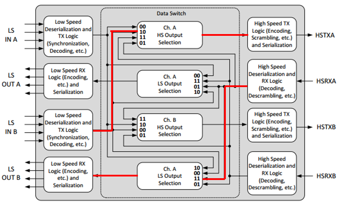
    3. The Data Switch block is not built-in neither low or high speed side, basically this block is independent for every side. So, for the transmit path (LSINB ==> HSOUTA verify the data switch in channel A), for the receive path (HSRXA ==> LSOUTB verify data switch in Channel B).


    CHANNEL_STATUS_1 Channel A & B, since this register includes low and high speed, so, check low speed for CHB and high speed for CHA, I mean, in channel B you should verify LS_ALIGN_STATUS, LS_PLL_LOCK and in Channel A check HS_LOS, HS_AZ_DONE, HS_AGC_LOCKED, etc.
    LS_STATUS_1 Channel B
    PCS_STATUS_1 Channel A
    HS_ERROR COUNTER Channel A

    Best Regards,
    Luis
  • Hi Luis-san,

    Fortunately, We could establish the link through LSA to HSB using the setting as you mentioned.The reason for not linking properly was in the XAUI source. After fixing FPGA code, we finally see asserted  LS_ALIGN_STATUS bit.

    Thanks for taking your time on this.
    Could you double check if the each status below is as you expected just in case?

    Channel A(Using High side)
    CHANNEL_STATUS_1 0x00F 1C03
    PMA_STATUS_1 0x001 0006
    PMA_STATUS_2 0x008 B000
    PCS_STATUS_1 0x001 0006
    PCS_STATUS_2 0x008 8001

    Channel B(Using Low side)
    CHANNEL_STATUS_1 0x00F 7003
    LS_STATUS_1 0x015 C143

    As the result, We understood that ChA's PMA and PCS status should be referred to check the operation properly in the case(LSB to HSA switching). 

    1. [Switching initialized issue]
    But the issue that the switch is initialized arbitrarily has not been solved yet. It seems that the issue occurs when TLK10232 gets "local fault" due to some reason such as OPT cable unplug.

    So We are guessing ON_OFF feature in data switching control is related to this issue. We were looking for the register to disable the ON_OFF feature and reached out the registers below.

    DST_FORCE_SEL[4:0]
    DSR_FORCE_SEL[4:0]

    In fact, We succeeded in solving this problem by setting the registers.

    Channel A
    0x0017 2014
    0x0018 AC20(Might not be necessary)
    0x0019 2512
    0x001A 6C20(Might not be necessary)
    Channel B
    0x0017 2018
    0x0018 CC20(Might not be necessary)
    0x0019 2518
    0x001A EC20(Might not be necessary)

    We realized that these registers can force switch setting uniquely, Is this understanding correct?

    And please let me know if there are any note to use this registers. 

    Regards,

    Takashi Onawa

  • Hi Luis-san,

    My customer needs to fix their software soon.

    Could you give me any comments for questions above?

    Especially, we would like to know how the registers below behaves and whether our understanding is correct or not..

    DST_FORCE_SEL[4:0]
    DSR_FORCE_SEL[4:0]

    Regards,
    Takashi Onawa
  • Hi Takashi-san,

    The DST_FORCE_SEL[4:0] handles the manual data switch control. Basically this RESERVED REGISTER has 2 behaviors:

    1. When DST_FORCE_SEL[4] is 1'b1, EN[3:0] value is equal to DST_FORCE_SEL[3:0].
    2. When DST_FORCE_SEL[4] is 1'b0, EN[3:0] value is set through data-switch control logic.

    I hope this helps.

    Regards,
    Luis
  • Hi Luis-san,

    I read its full manual and set the register but I didn't understood the two points below.
    a. Why is this register hidden? Although It looks very useful to force the switch setting.
    b. What is the difference between the manual switching and the normal switching below?

    /Setting for DATA Switch TX (LSB=>HSA direction) CONFIGURE CHANNEL A
    //To Ch-A phy address;
    Write 1'b0 to 0x1E.0017 bit 12 (DST_PIN_SW_EN)
    Write 2’b10 to 0x1E.0018 bits 15:14 (DST_DATA_SRC_SEL[1:0]) //Selects data from Low Speed CHB to High Speed CHA

    //Setting for DATA Switch RX (HSA=>LSB direction) CONFIGURE CHANNEL B
    //To Ch-A Ch-B phy address;
    Write 1'b0 to 0x1E.0019 bit 12 (DSR_PIN_SW_EN)
    Write 2’b11 to 0x1E.001A bits 15:14 (DSR_DATA_SRC_SEL[1:0]) //Selects data from alternate channel HS input

    Regards,
    Takashi Onawa
  • Hi Takashi-san,

    a. I agree, we need to fix the datasheet since there are several information that need to be updated to avoid "lacks" for the user.
    b. TLK10232 utilizes "smart switching" logic, which is "normal" switching. When a data-path is switched, it will wait until the current packet finishes, and then it will wait in Idle until the new path begins a packet. In this way, we never transmit a broken/corrupt packet. Manual switch will simply do on-the-fly switching and can result in data corruption.

    Best Regards,
    Luis