This thread has been locked.

If you have a related question, please click the "Ask a related question" button in the top right corner. The newly created question will be automatically linked to this question.

TCA9406 datasheet VIL question

Other Parts Discussed in Thread: TCA9406, TCA9517

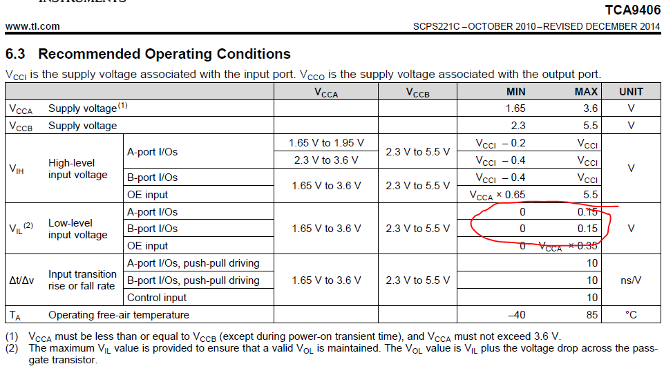
customer report the more devices's VOL might be higher than TCA9406 VIL spec define(0.15V max).Is there any risk in if another devices' VOL higher than VIL of TCA9406?  Is that the issue make the TCA9406 function/level conversion fail?

  • The VIL footnote says:

    The maximum VIL value is provided to ensure that a valid VOL is maintained. The VOL value is VIL plus the voltage drop across the pass-gate transistor.

    So a higher VIL would just increase the TCA9406's VOL.

    Furthermore, the VOL values in section 6.5 are specified at a current of 1 mA. The pass-gate transistor, when switched on, behaves pretty much like a resistor, so you can reduce its voltage drop by reducing the current through it; see section 6.12.

  • Hi Mr. Ladisch,

    So, does it mean the impedance of the turned-on pass-gate is (0.4V-0.15V)/1mA=250ohm? According to the datasheet, it specifies that the gate bias of the passgate is the voltage level of low voltage side plus the threshold voltage of the the passgate. As a result, is the impedance of the turned-on passgate with respect to the voltage level of low voltage side?

    Regards,
    S.P. Lin
  • Hi Support,

    Can you help answer me the question? I need the information to evaluate if that is feasible while we implement PCA9406 with another I2C repeater. I am worried about the voltage across the turned-on passgate impedance.

    Regards,
    S.P. Lin
  • I don't know why the datasheet mentions the threshold voltage; you don't know it, and it is not relevant. Ignore it.

    The worst-case impedance can indeed be computed as above. (Section 6.12 shows that the typical impedance is near 25 ohms, but that is not guaranteed.)
  • Hi Mr. Ladisch,

    I just attached the calculation procedure for both the turned-on impedance of PCA9406's passgate and the pull-down driver impedance of the device.

    And as per my calculation, I thought there might be something wrong. Can you help to confirm the attachment?

    And also, during my calculation, I am a little confused about the definition of I/O's sink ability. Does the sink ability mean there is a current source draw the current into the device and generally it can draw about 3mA?

    As my original understanding, I think the turned on pull-down driver can just be simplified as a resistor and the maximum sink current means the current will cause the maximum VOL as spec. shown.

    Is there any misunderstanding? Please correct me if my original thought is wrong. Thanks a lot.

  • Hi there supporter,

    Can you help answer the questions? I am looking forward your response.
    Thanks.

    Regards,
    S.P. Lin
  • Part of i1 flows through the right pull-up resistors, not from the output.

    I do not understand why you ask about "the definition of I/O's sink ability". The datasheet specifies VOL for certain test conditions; if your input driver results in different currents/voltages at the input, then VOL will be different.
  • Hi Mr. Ladisch,

    The questions I raised on the last two posts are just to confirm whether the turned-on impedance of TCA9406 is static 25-ohm and it is not a dynamic value. Can you help to confirm that? And also, the datasheet says it is recommended to reserve external pull-up resistors for TCA9406. However, as I know, TCA9406 has one-shot for rising edge and the turned on impedance is around 70ohm. So, I think the external pull-up resistors maybe not necessary. Is there any misunderstanding? Or, are the pullup any specific functions that I never think of?

    Regards,
    S.P. Lin
  • A switched-on FET (here: the pass-gate transistor) behaves mostly like a (static) resistor.

    The datasheet says:

    The TCA9406 features internal 10-kΩ pullup resistors on SCL_A, SDA_A, SCL_B, and SDA_B. Additional external pullup resistors can be added to the bus to reduce the total pullup resistance and speed up rising edges.

  • Hello S.P. Lin,
    The one shot is only turned on for a short period of time to help the rising edge get to it's final voltage level as quickly as possible. The selection of the pull up resistor depends on many variables. You need to consider the voltage levels, the amount of capacitance (which includes the number of devices on the bus and the trace capacitance), and the frequency you wish to operate at. The internal 10k ohms is fixed but may need to be reduced to achieve your system level goals. This can be done by adding an external resistor. That is why we generally recommend at least having a place holder for it in your design. If you go through the calculations you may find out that you don't need it, but I generally like to have the pull-up place holders there as back up. Do you have very strict form factor requirements that don't allow you to have the pull-up resistors place on your design?
    -Francis Houde
  • Hi Francis,

    It is really weird that: according to the table of datasheet 6.5, the worst case for VOL of both sides would be 0.4V@1mA. And the test condition for VCCA is within 1.65V to 3.3V whereas for VCCB is within 2.3V to 5.5V. However, after checking the figures of datasheet 6.12, it is hard to say why only 1mA will cause the VOL go to 0.4V. I am thinking maybe that is because 6.12 is showing the typical characteristics but 0.4V VOL is just for the worst. Nevertheless, I sill need you help to clarify that: in what kind of case that VOL will go to 0.4V when IOL is around 1mA and VIL is not greater than 0.15V?

    Your kindly help will be appreciated.

    Regards,
    S.P. Lin
  • Hi Francis,

    The products our company making are specific for industrial. Therefore, to support extended temperature, -40~85 degree C, is required.

    And seeing the datasheet figure 6.5, I just find the maximum 0.4V VOL is specified in the column for -40~85 degree C.

    Since Rds(on) is proportional to temperature, does it mean the maximum 0.4V VOL will happen at the maximum supported temperature 85 degree C?

    And here I just put a evaluation procedure for a common case, and please help to review it and let me know if you have any comment. 

    I'm looking forward your response. Your kindly help will be appreciated.

    Regards,

    S.P. Lin

  • Hi Francis,

    I am trying to calculate the worst case as spec. shows. Please see below circuit which just follows the test conditions specified.

    As you can see, if VCCB(min)= 2.3V, to make VOL=0.4V the current drawn would be 0.19mA. And if VCCB(MAX)=5.5V, to make VOL=0.4V the current drawn should be 0.51mA.

    And 1mA is not within 0.19~0.51mA. Is there anything wrong? Can you help to confirm this question first?

    Your kindly help will be appreciated.

    Regards,

    S.P. Lin

  • Hi Francis,

    Do you have any comment for this?

    Regards,
    S.P. Lin
  • Hi Francis and all supporters who can help answer these questions,


    All the questions I asked in this thread are not only for technical or interest but for business. Our company is now trying to define the standard solutions for all the applications and make too many types of IC solutions used by our products much simpler. Thus, we have to well know the pros and cons among a variety of similar solution as well as their working principle since we believe it will help us pick up the best configuration. And TI is the best IC manufacturer to me because TI has this forum and lots of experts here to answer our questions. However, we still need efficient response. If we can get the response earlier, we can make decision quickly.

    The sooner we make the decision, the earlier we buy in the IC solutions. That is what I said, the business.


    And the questions I asked on the previous posts are trying to verify which level shifter solution is the best one in order to translate the voltage level between 1.8V and 3.3V, especially for a DP++ port with DDC channel which goes from Intel Atom series chipset to a HDMI active level shifter, such as TI’s DP139 and NXP’s PTN3360/61, in an external dongle device.


    Usually, the HDMI active level shifter assigns the side with static offset voltage to 3V side, which is also called source side. So, if we use TCA9517 as a solution for host chipset’s 1.8V I/O and DP139’s 3V source side, and configure its B-side to 3V side, possibly it would have problems because the low from TCA9517’s B-side is not low enough to meet the contention voltage requirement of DP139. And if we assign TCA9517’s A-side to DP139’s 3V source side and let B-side connected to host chipset, since the maximum input low voltage is 1.8V*0.35=0.63V, the maximum output low from TCA9517 is up to 0.6V which is too close to 0.63V.


    As we turn to use TCA9406, below shows the calculation results based upon different configuration. And there is one thing we should pay attention to that: most of DP to HDMI passive dongles follow the manufacturer’s reference design to put the external pullups close to the active HDMI level shifter. So, here the equivalent resistance for TCA9406’s A-side and B-side would include TCA9406’s internal pullups, 10-kohm external pullups and 2.2-kohm on HDMI passive dongle. And according to below calculation results, it seems, even though to use the simplest configuration of TCA9406, B-side low would violate the input contention voltage requirement of the built-in level translator for DDC at 85 degree Celsius ambient temperature. Can you help point out is there anything wrong on the evaluation for TCA9406? And also, if the thoughts are correct, do you have any recommended solution for this application? Now, we are considering to use TCA9617 which has a little lower maximum VOL, 0.58V. But I still think it is not low enough.

    Regards,

    S.P. Lin

  • Hello S.P.Lin,
     

    Sorry for the delay in response. Thank you for putting the effort to a good post. I initially didn't realize that this post was specifically for DDC in HDMI applications. Generally speaking we have recommended people using the TCA9517.


    I am only marginally knowledgeable about the HDMI DDC compliance testing and was hoping you could confirm a few things with respect to the specifications. It is my understanding that you need to minimize the capacitance on the DDC lines to make sure the max capacitance level is not exceeded. If that is the case, then it would mean that you should probably be using a buffered translator, which will perform the translation/level shifting and also isolate the capacitances from each side of where the buffer is located. You should stay away from PASS FET types of translators/level shifters because it doesn’t provide the capacitive isolation. Unless you can make sure the total capacitances are within range, then a PASS FET translator might work. This is why I would not recommend using the TCA9406 and would recommend using something like the TCA9517, which is a true buffer.


    It has been my experience that the method of doing the capacitive load testing outline in the HDMI specifications is problematic. The specifications define the LCR test signal, which I believe is a 1 or 100kHz sinusoid that has a peak to peak voltage of 2.5V with a 2.5V DC bias offset.


    When using this measurement tool while the part is active, the LCR meter will get an incorrect capacitance measurement, because during the measurement the AC signal can interact with the circuitry and change what the perceived impedance is to the LCR meter. Instead of measuring the impedance due to purely capacitive load, the meter will record the impedance from the capacitive load and the active circuitry such as the rise time accelerators, or static voltage offsets. To the meter is looks like a lower impedance therefore it must be larger capacitive load, when in fact that isn’t true. If the setting of the meter were changed or the method of the capacitance measurement was done differently, then the errors wouldn’t be seen when doing the capacitance compliance testing.


    The TCA9517 has been used in the past for HDMI DDC channel.


    My only recommendation is to do 1 of the following:


    1) Connect the A side of the TCA9517 to the HDMI cable if possible (static voltage offset can caused weird issues with compliance test, and doing this will avoid those measurement errors).


    2) Have a detection scheme that will pull EN to GND while doing compliance testing. This disables the active circuitry and therefore allows for the measurement of the true capacitive loading.


    Can you help me understand your diagram. Can you draw me what the HDMI-DDC source is (along with source voltage range), can you draw what the HDMI-DDC sink is along with it’s voltage range? Where is the cable? What is the node where the capacitive load compliance test is performed? Can you show me where all the pullups are in the system?


    Is the source side generally the higher voltage? I need to look up the DP139 to understand the Vil requirements. In your post you speak about the “host chipset”, can you explain what that means? Is this the source or sink?


    One more question, why isn't 30mV of tolerance enough?  Do you have a specific goal or target?

    -Francis Houde


    .

  • Hi Francis,

    What is the maximum VIL that can still let TCA9406's internal passgate turned on?

    Regards,
    S.P. Lin
  • Hello S.P. Lin,

    The maximum VIL is 0.15V, but keep in mind that this is over all process and temp.

    Francis Houde 

  • Hi Francis,

    According to I2C base spec., the maximum VOL value of I2C devices is specified as 0.4V. If the 0.15V you pointed out is the maximum acceptable low level that can make TCA9406's internal passgate turned on, it means TCA9406 cannot be applied to most of I2C devices, right? Additionally, the footnote under the table you extracted shows that "The maximum VIL value is provided to ensure that a valid VOL is maintained". So, my understanding is this VIL(MAX)=0.15V is not the necessary condition to let TCA9406's internal passgate turned-on.
    Therefore, can you let me know the VGS(th) of the internal passgate?

    Regards,
    S.P. Lin
  • Hi Francis,

    I just forgot to say what I am concerned about is in case of the same level is applied to the both sides of TCA9406.

    Regards,
    S.P. Lin
  • Hi Francis,

    Do you have any information for my question? I'm looking forward your replies.
    Thanks.

    Regards,
    S.P.