This thread has been locked.

If you have a related question, please click the "Ask a related question" button in the top right corner. The newly created question will be automatically linked to this question.

RM48L952: RAM divided over multiple banks

Part Number: RM48L952

Hello there,

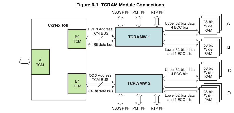
The following picture from the RM48x technical reference manual (SPNU503B – November 2012 – Revised August 2013 p 297) raises some questions.
Here is what I know and understand:

  • Only one of the two Cortex R4F's is drawn, the second one also has its own B0TCM and B1TCM.
  • From the ARM Cortex-R4F technical reference manual I found that a single R4F is allowed to have two BTCM interfaces, these BTCM interfaces are interleaved on either
    • Bit[3] of the address
    • On the MSB
  • The RM48L952 has two RAM bank

Now the following sentence of the RM48L952 datasheet ( SPNS177D – SEPTEMBER 2011 – REVISED JUNE 2015 p 85) confuses me.
Features of the TCRAM :
"Provides enhanced safety for the RAM addressing by implementing two 36-bit-wide byte-interleaved RAM banks
and generating independent RAM access control signals to the two banks"

On the picture however i see 4 36-bit wide RAMS (I labeled them A, B, C, D).
I do not understand the relation between this picture and sentence I quoted.
A couple of concrete questions:
1) How many RAM banks are there?

2) How are A, B, C and D fit into these banks?

3) If I declare a uint8_t array[16] = {0x00, 0x11, 0x22, 0x33, 0x44 .. 0xFF};
How is this stored into / divided over the memory banks (or regions? ABCD)?

Thanks in advance,

Best regards.

Karel

  • Hi Karel,

    See my comments below:

    • Only one of the two Cortex R4F's is drawn, the second one also has its own B0TCM and B1TCM.

      >> Only one of the two Cortex R4F's outputs are connected to the TCM interconnect. The outputs from the second R4F are only connected to the CPU Compare Module (CCM).

    • From the ARM Cortex-R4F technical reference manual I found that a single R4F is allowed to have two BTCM interfaces, these BTCM interfaces are interleaved on either
      • Bit[3] of the address
      • On the MSB

        >> The two BTCM interfaces are interleaved on a 64-bit boundary. So every consecutive 64-bit read occurs from a different BxTCM. This allows multiple bus masters (e.g. CPU, DMA) to access the CPU RAM in parallel, as long as they don't access the same 64-bit address.

    • The RM48L952 has two RAM bank

    >> The RM48L952 has 256KB of RAM, which is physically broken up into 16 banks of 16KB each. Each BxTCM interface addresses eight 16KB banks.

    Within each BxTCM, there are two physical 36-bit banks that are 32-bit interleaved. This is done so that any bit-disturb source (e.g. neutron) does not affect more than 1 bit within a 64-bit value.

    Hope this helps.

    Regards, Sunil

  • Thanks for your reply.

    If I understand correctly an array of 16 bytes {0x00, 0x11, 0x22, ... 0xFF} would be stored in the following way

    Value Address offset
    0x00 0
    0x11 1
    0x22 2
    0x33 3
    0x44 4
    0x55 5
    0x66 6
    0x77 7
    0x88 8
    0x99 9
    0xaa a
    0xbb b
    0xcc c
    0xdd d
    0xee e
    0xff f

    0x00 ... 0x77 would be passed via B0TCM, 0x88 ... 0xFF via B1TCM.

    TCRAMW1 then places 0x00..0x33 in one RAM bank (R1) and 0x44..0x77 in another RAM bank (R2)

    TCRAMW2 then places 0x88..0xBB in one RAM bank (R3) and 0xCC..0xFF in another RAM bank (R4)

    R1,R2,R3 and R4 are all different RAM banks (ABCD on my picture)

    Is this correct?

    Thanks

  • Karel,

    Yes this is correct. The application or the CPU does not really get to individually identify each RAM bank separately, as the implementation has no impact on a CPU read or write operations. These implementation details are just highlighted in the manual to communicate the benefits of the implementation: better SRAM bandwidth in case of parallel accesses, and increased robustness for bit-disturbs.

    Regards,
    Sunil