


Hi,
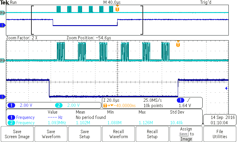
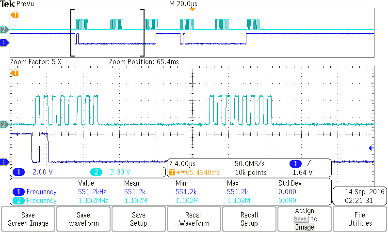
I'm interfacing MSP430F5529 launchpad with ADS1248 via SPI. I was monitoring the UCB0TXBUF and RXBUF registers while running CCS and found that only TXBUF is getting the values and RXBUF always return 0x00 whenever a register is read. I first want to have a setup where I can write and read back registers properly. Upon seeing the waveforms of SPI on DSO, I found that the SCLK gets turned off whenever RXBUF is being used to read data. Please help in solving this issue. Please find the attachments of code and the waveforms below.
#include <msp430.h>
#include "ADS_settings.h"

void config_CLOCK(void); //8MHz
void CONFIG_SPI_ADS(void); //UCB0 as SPI


unsigned char REG_ADDR[15] = {MUX0,VBIAS,MUX1,SYS0,OFC0,OFC1,OFC2,FSC0,FSC1,FSC2,IDAC0,IDAC1,GPIOCFG,GPIOCDIR,GPIODAT};
unsigned char REG_VAL[15]= {MUX0_VAL,VBIAS_VAL,MUX1_VAL,SYS0_VAL,OFC0_VAL,OFC1_VAL,OFC2_VAL,FSC0_VAL,FSC1_VAL,FSC2_VAL,IDAC0_VAL,IDAC1_VAL,GPIOCFG_VAL,GPIOCDIR_VAL,GPIODAT_VAL};
unsigned char READ_REG[15]={0x00};
unsigned char read_data = 0;
unsigned char dummy = 0;
int main(void)
{
    WDTCTL = WDTPW | WDTHOLD;	// Stop watchdog timer
    config_CLOCK();

    CONFIG_SPI_ADS();
    //__bis_SR_register(GIE); //enable interrupts
    __delay_cycles(10000);
    P2OUT &= ~ BIT5; //RESET pin low - resets digital circuits
    __delay_cycles(100000);
       P2OUT |= BIT5;              //RESET high
       P2OUT |= BIT6;				//CS high
       P2OUT |= BIT4;              //Make START pin as HIGH
while(1)
{

    P2OUT &= ~BIT6;	//Make CS low

    while (!(UCB0IFG & UCTXIFG)); 			// Make sure nothing is already in the TX buffer
    UCB0TXBUF = 0x40;					// Send the write commmand with 0x00 as start address
   	while (!(UCB0IFG & UCRXIFG)); 			// Before returning wait until transmission is complete
   	dummy = UCB0RXBUF;

    while (!(UCB0IFG & UCTXIFG)); 			// Make sure nothing is already in the TX buffer
   	UCB0TXBUF = 0x00;					// Send the no. of registers to be written
   	while (!(UCB0IFG & UCRXIFG)); 			// Before returning wait until transmission is complete
   	dummy = UCB0RXBUF;

    while (!(UCB0IFG & UCTXIFG)); 			// Make sure nothing is already in the TX buffer
   	UCB0TXBUF = 0x01;					// Send the register value
   	while (!(UCB0IFG & UCRXIFG)); 			// Before returning wait until transmission is complete
   	dummy = UCB0RXBUF;


    while (!(UCB0IFG & UCTXIFG)); 			// Make sure nothing is already in the TX buffer
   	UCB0TXBUF = 0x20;					// Send the read register command
   	while (!(UCB0IFG & UCRXIFG)); 			// Before returning wait until transmission is complete
   	UCB0IFG &= ~(UCRXIFG);
   	dummy = UCB0RXBUF;

    while (!(UCB0IFG & UCTXIFG)); 			// Make sure nothing is already in the TX buffer
   	UCB0TXBUF = 0x00;					// Send the no.of registers to read
   	while (!(UCB0IFG & UCRXIFG)); 			// Before returning wait until transmission is complete
   	dummy = UCB0RXBUF;

    while (!(UCB0IFG & UCTXIFG)); 			// Make sure nothing is already in the TX buffer
   	UCB0TXBUF = 0xFF;					// Send dummy Byte to take data from register
   	while (!(UCB0IFG & UCRXIFG)); 			// Before returning wait until transmission is complete
   	read_data = UCB0RXBUF;                           //store the register value

   	P2OUT |= BIT6;	//Make CS high
   	__delay_cycles(10000);
}

}
void config_CLOCK(void)  //SMCLK CONFIGURAATION
{
  volatile unsigned int i;

  P1DIR |= BIT1;                            // P1.1 output
  P1DIR |= BIT0;                            // ACLK set out to pins
  P1SEL |= BIT0;
  P2DIR |= BIT2;                            // SMCLK set out to pins
  P2SEL |= BIT2;
  P7DIR |= BIT7;                            // MCLK set out to pins
  P7SEL |= BIT7;

  UCSCTL3 = SELREF_2;                       // Set DCO FLL reference = REFO
  UCSCTL4 |= SELA_2;                        // Set ACLK = REFO
  UCSCTL0 = 0x0000;                         // Set lowest possible DCOx, MODx

  // Loop until XT1,XT2 & DCO stabilizes - In this case only DCO has to stabilize
  do
  {
    UCSCTL7 &= ~(XT2OFFG + XT1LFOFFG + DCOFFG);
                                            // Clear XT2,XT1,DCO fault flags
    SFRIFG1 &= ~OFIFG;                      // Clear fault flags
  }while (SFRIFG1&OFIFG);                   // Test oscillator fault flag

  __bis_SR_register(SCG0);                  // Disable the FLL control loop
  UCSCTL1 = DCORSEL_5;                      // Select DCO range 16MHz operation
  UCSCTL2 |= 15;
                                            // (N + 1) * FLLRef = Fdco

  __bic_SR_register(SCG0);                  // Enable the FLL control loop

  // Worst-case settling time for the DCO when the DCO range bits have been
  // changed is n x 32 x 32 x f_MCLK / f_FLL_reference. See UCS chapter in 5xx
  // UG for optimization.
  // 32 x 32 x 8 MHz / 32,768 Hz = 250000 = MCLK cycles for DCO to settle
  __delay_cycles(250000);

  }

void CONFIG_SPI_ADS(void)  //SPI initialization
{
    UCB0CTL1 |= UCSWRST;                            //set software reset to 1 so we can configure SPI

    //UCB0STAT |= UCLISTEN;                           //the launchpad listens to itself (use for testing)
    UCB0CTL0 |= UCCKPH+UCMSB + UCMST + UCSYNC;    //clkphase,clkpolarity,MSBfirst,8-bit,master mode, 3-pin, synchronous SPI
    UCB0CTL1 |= UCSSEL_2;                           //choose SMCLK as our clock. SMCLK is 1.1 MHz. We divise it with the baud register
    UCB0BR0 |= 0x02;                                //Prescalar for the SCLK (2 bytes). Here it sets 8MHz sclk to 4MHz
    UCB0BR1 = 0;                                    //upper byte of br register. set to zero
    __delay_cycles(10);

    P1DIR &= ~BIT1; //DRDY - Input to MCU
    P2DIR |= BIT4; //START - Output from  MCU
    P2DIR |= BIT5; //RESET - Output from  MCU
    P2DIR  |= BIT6;  //CS - Output from MCU
    P3DIR |= BIT0+BIT2; //3.0-MOSI, 3.2-SCLK Output from MCU
    P3DIR &= ~BIT1;     //3.1 MISO Input to MCU

    P3SEL |= (BIT0 | BIT1 | BIT2);  //configures pins for three pin SPI. MISO P3.1, MOSI P3.0, SCLK P3.2


    __delay_cycles(10);
    UCB0CTL1 &= ~UCSWRST;                   //enables the SPI to work
    UCB0IE |= UCTXIE+UCRXIE;                        // Enable USCI0 TX AND RX interrupt
}
SCLK (2) - CS (1) SIGNALS:

SCLK (2) - MOSI (1) SIGNALS:

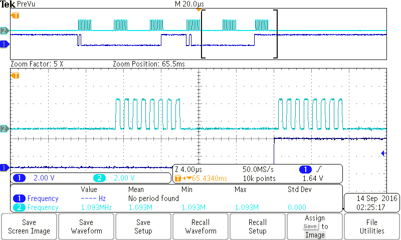
SCLK (2)- MISO (1) SIGNALS:


Please let me know if further information is required.
Thanks & Regards,
Vignesh


