This thread has been locked.

If you have a related question, please click the "Ask a related question" button in the top right corner. The newly created question will be automatically linked to this question.

CCS/MSP432P401R: Trouble with SPI using DMA

Part Number: MSP432P401R

Tool/software: Code Composer Studio

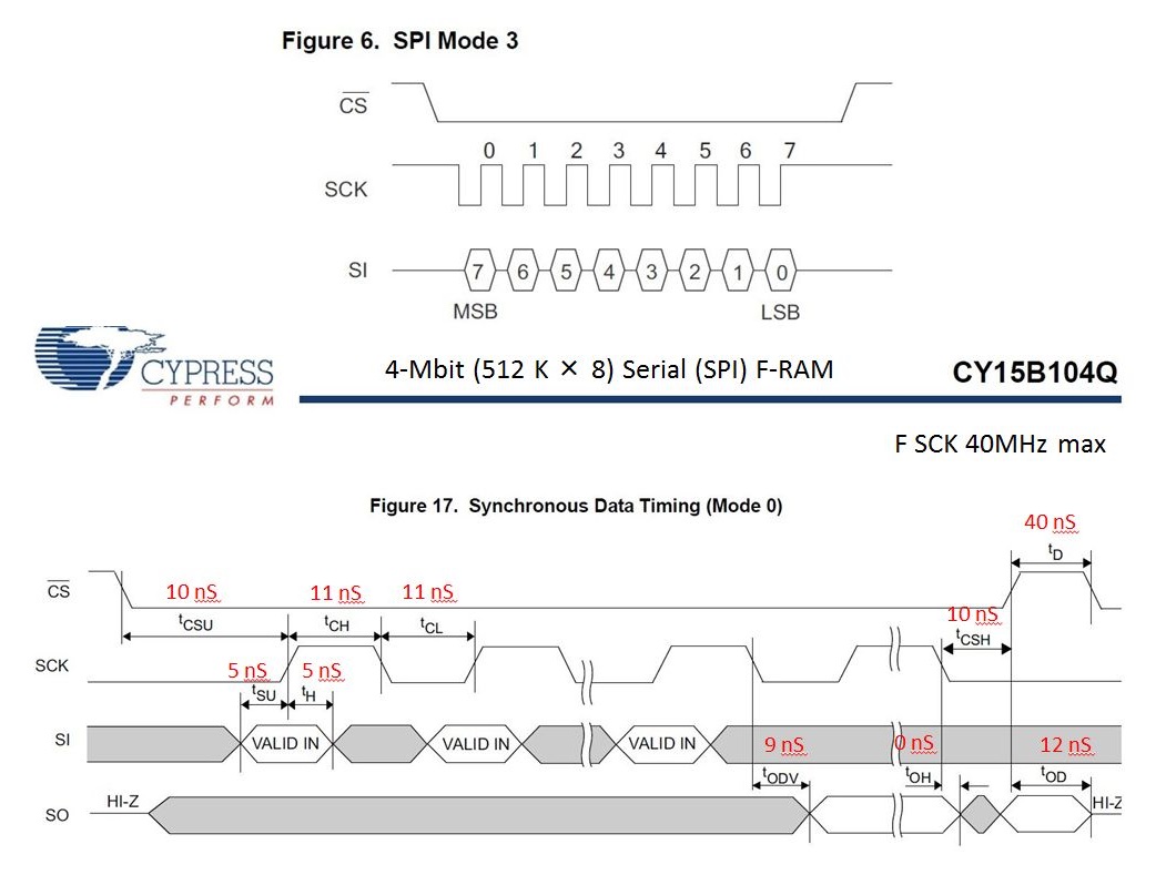
I attached FRAM with SPI to EUSCI_B0.

I configured the SPI port as follows.

// Configure SPI interface
EUSCI_B0->CTLW0 |= EUSCI_B_CTLW0_SWRST; // Put eUSCI state machine in reset
EUSCI_B0->CTLW0 = EUSCI_B_CTLW0_SWRST | // Remain eUSCI state machine in reset
EUSCI_B_CTLW0_MST | // Set as SPI master
EUSCI_B_CTLW0_SYNC | // Set as synchronous mode
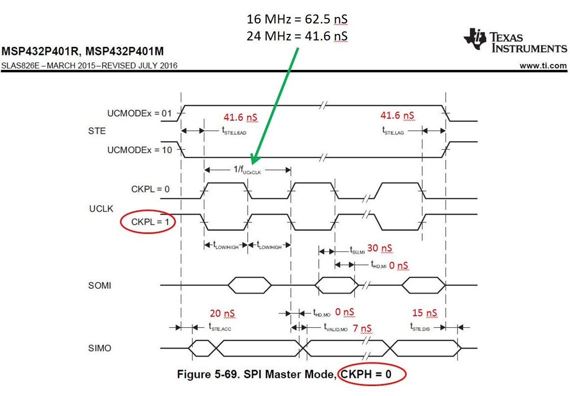
EUSCI_B_CTLW0_CKPL | // Set clock polarity high
EUSCI_B_CTLW0_MSB; // MSB first

EUSCI_B0->CTLW0 |= EUSCI_B_CTLW0_SSEL__SMCLK; // SMCLK=24MHz 2017-2-21
EUSCI_B0->BRW = 0x00; // fBitClock = fBRCLK/(UCBRx+1). 0 = 24MHz CLK 2017-2-23
EUSCI_B0->CTLW0 &= ~EUSCI_B_CTLW0_SWRST;// Initialize USCI state machine


I tried to write 256 data = 512 byte to FRAM as below.

int i;
int16_t fram_data = 0; // 16bit data for FRAM
uint32_t d1;


for(i=0; i<256 ; i++)
{
d1 = (fram_data >> 8) & 0x0ff;
while (!(EUSCI_B0->IFG & EUSCI_B_IFG_TXIFG));
EUSCI_B0->TXBUF = d1; // data b15 to b8
while (!(EUSCI_B0->IFG & EUSCI_B_IFG_RXIFG));
IDdata = EUSCI_B0->RXBUF;

d1 = fram_data & 0x0ff;
while (!(EUSCI_B0->IFG & EUSCI_B_IFG_TXIFG));
EUSCI_B0->TXBUF = d1; // data b7 to b0
while (!(EUSCI_B0->IFG & EUSCI_B_IFG_RXIFG));
IDdata = EUSCI_B0->RXBUF;

fram_data++;
}

This way, I can write the Data all right.

(I use back channel UART to dump the FRAM data.)

fram_data = 0800 to 0900 = 256 data written
fram_read_data =
0800 0801 0802 0803 0804 0805 0806 0807 0808 0809 080A 080B 080C 080D 080E 080F
0810 0811 0812 0813 0814 0815 0816 0817 0818 0819 081A 081B 081C 081D 081E 081F
0820 0821 0822 0823 0824 0825 0826 0827 0828 0829 082A 082B 082C 082D 082E 082F
0830 0831 0832 0833 0834 0835 0836 0837 0838 0839 083A 083B 083C 083D 083E 083F
0840 0841 0842 0843 0844 0845 0846 0847 0848 0849 084A 084B 084C 084D 084E 084F
0850 0851 0852 0853 0854 0855 0856 0857 0858 0859 085A 085B 085C 085D 085E 085F
0860 0861 0862 0863 0864 0865 0866 0867 0868 0869 086A 086B 086C 086D 086E 086F
0870 0871 0872 0873 0874 0875 0876 0877 0878 0879 087A 087B 087C 087D 087E 087F
0880 0881 0882 0883 0884 0885 0886 0887 0888 0889 088A 088B 088C 088D 088E 088F
0890 0891 0892 0893 0894 0895 0896 0897 0898 0899 089A 089B 089C 089D 089E 089F
08A0 08A1 08A2 08A3 08A4 08A5 08A6 08A7 08A8 08A9 08AA 08AB 08AC 08AD 08AE 08AF
08B0 08B1 08B2 08B3 08B4 08B5 08B6 08B7 08B8 08B9 08BA 08BB 08BC 08BD 08BE 08BF
08C0 08C1 08C2 08C3 08C4 08C5 08C6 08C7 08C8 08C9 08CA 08CB 08CC 08CD 08CE 08CF
08D0 08D1 08D2 08D3 08D4 08D5 08D6 08D7 08D8 08D9 08DA 08DB 08DC 08DD 08DE 08DF
08E0 08E1 08E2 08E3 08E4 08E5 08E6 08E7 08E8 08E9 08EA 08EB 08EC 08ED 08EE 08EF
08F0 08F1 08F2 08F3 08F4 08F5 08F6 08F7 08F8 08F9 08FA 08FB 08FC 08FD 08FE 08FF


But, when I try to write the same data using DMA as below,

#pragma DATA_ALIGN(d8, 512)
union DATA16B8B {
uint16_t d16[256];
uint8_t d8[512];
};

union DATA16B8B data16b8b;

void SPI_fram_write_dma( uint8_t mstxData[], int n )
{
/* Assign DMA channel 0 to EUSCI_B0_TX0, channel 1 to EUSCI_B0_RX0 */
MAP_DMA_assignChannel(DMA_CH0_EUSCIB0TX0);

/* Setup the TX transfer characteristics & buffers */
MAP_DMA_setChannelControl(DMA_CH0_EUSCIB0TX0 | UDMA_PRI_SELECT,
UDMA_SIZE_8 | UDMA_SRC_INC_8 | UDMA_DST_INC_NONE | UDMA_ARB_1);
MAP_DMA_setChannelTransfer(DMA_CH0_EUSCIB0TX0 | UDMA_PRI_SELECT,
UDMA_MODE_BASIC, mstxData,
(void *) MAP_SPI_getTransmitBufferAddressForDMA(EUSCI_B0_BASE),
n);
MAP_DMA_enableChannel(0);
}

for(i=0; i<256 ; i++)
{
data16b8b.d16[i] = fram_data;
fram_data++;
}

SPI_fram_write_dma(&data16b8b.d8[0], 512);


Some part of the data looks all right, but there are a lot of strange data.

fram_data = 0900 to 0A00 = 256 data written
fram_read_data =
0000 0901 0902 0903 0904 0905 0906 0907 0908 0909 090A 090B 090C 090D 090E 090F
0910 0911 0912 0913 0914 0915 0916 0917 0918 0919 091A 091B 091C 091D 091E 091F
0920 0921 0922 0923 0924 0925 0926 0927 0928 0929 092A 092B 092C 092D 092E 092F
0930 0931 0932 0933 0934 0935 0936 0937 0938 0939 093A 093B 093C 093D 093E 093F
0940 0941 0942 0943 0944 0945 0946 0947 0948 0949 094A 094B 094C 094D 094E 094F
0950 0951 0952 0953 0954 0955 0956 0957 0958 0959 095A 095B 095C 095D 095E 095F
0960 0961 0962 0963 0964 0965 0966 0967 0968 0969 096A 096B 096C 096D 096E 096F
0970 0971 0972 0973 0974 0975 0976 0977 0978 0979 097A 097B 097C 097D 097E 097F
0980 0981 0982 0983 0984 0985 0986 0987 0988 0989 098A 098B 098C 098D 098E 098F
0990 0991 0992 0993 0994 0995 0996 0997 0998 0999 099A 099B 099C 099D 099E 099F
09A0 09A1 09A2 09A3 09A4 09A5 09A6 09A7 09A8 09A9 09AA 09AB 09AC 09AD 09AE 09AF
09B0 09B1 09B2 09B3 09B4 09B5 09B6 09B7 09B8 09B9 09BA 09BB 09BC 09BD BE09 BF09
C009 C109 C209 C309 C409 C509 C609 C709 C809 C909 CA09 CB09 CC09 CD09 CE09 CF09
D009 D109 D209 D309 D409 D509 D609 D709 D809 D909 DA09 DB09 DC09 DD09 DE09 DF09
E009 E109 E209 E309 E409 E509 E609 E709 E809 E909 EA09 EB09 EC09 ED09 EE09 EF09
F009 F109 F209 F309 F409 F509 F609 F709 F809 F909 FA09 FB09 FC09 FD09 FE09 FF09

What should I do now?

  • Hello,
    I would recommend first trying to use a slower clock speed and no DMA to make sure that the issue is with the DMA configuration and not the SPI settings. Once you have a slower speed configuration working then add DMA and then finally increase to the desired speed.

    Regards,
    Chris
  • I did !

    I tried at about 16kHz clock without DMA. 

    It worked all right. (Both write and read)

    I changed the frequency to 12MHz without DMA.

    It worked all right. (Both write and read)

    Now, I tried DMA, got strange result, and wondering. 

    I changed the write part using DMA. 

    So, there is something wrong with my DMA program. 

    Or something to do with "volatile" again?

    May be I should check the wave form at the FRAM input. 

    Hope to receive some answer soon!

  • DMA_SPI_TX_01.c
    /* --COPYRIGHT--,BSD_EX
     * Copyright (c) 2013, Texas Instruments Incorporated
     * All rights reserved.
     *
     * Redistribution and use in source and binary forms, with or without
     * modification, are permitted provided that the following conditions
     * are met:
     *
     * *  Redistributions of source code must retain the above copyright
     *    notice, this list of conditions and the following disclaimer.
     *
     * *  Redistributions in binary form must reproduce the above copyright
     *    notice, this list of conditions and the following disclaimer in the
     *    documentation and/or other materials provided with the distribution.
     *
     * *  Neither the name of Texas Instruments Incorporated nor the names of
     *    its contributors may be used to endorse or promote products derived
     *    from this software without specific prior written permission.
     *
     * THIS SOFTWARE IS PROVIDED BY THE COPYRIGHT HOLDERS AND CONTRIBUTORS "AS IS"
     * AND ANY EXPRESS OR IMPLIED WARRANTIES, INCLUDING, BUT NOT LIMITED TO,
     * THE IMPLIED WARRANTIES OF MERCHANTABILITY AND FITNESS FOR A PARTICULAR
     * PURPOSE ARE DISCLAIMED. IN NO EVENT SHALL THE COPYRIGHT OWNER OR
     * CONTRIBUTORS BE LIABLE FOR ANY DIRECT, INDIRECT, INCIDENTAL, SPECIAL,
     * EXEMPLARY, OR CONSEQUENTIAL DAMAGES (INCLUDING, BUT NOT LIMITED TO,
     * PROCUREMENT OF SUBSTITUTE GOODS OR SERVICES; LOSS OF USE, DATA, OR PROFITS;
     * OR BUSINESS INTERRUPTION) HOWEVER CAUSED AND ON ANY THEORY OF LIABILITY,
     * WHETHER IN CONTRACT, STRICT LIABILITY, OR TORT (INCLUDING NEGLIGENCE OR
     * OTHERWISE) ARISING IN ANY WAY OUT OF THE USE OF THIS SOFTWARE,
     * EVEN IF ADVISED OF THE POSSIBILITY OF SUCH DAMAGE.
     *
     * --/COPYRIGHT--
     */
    
    #include <ti/devices/msp432p4xx/inc/msp.h>
    #include <ti/devices/msp432p4xx/driverlib/driverlib.h>
    #include <stdio.h>
    
    /* Standard Includes */
    #include <stdint.h>
    #include <string.h>
    
    
    /* Clock system frequencies */
    /* Clock system frequencies */
    #define MCLK_FREQUENCY      32000000
    #define SMCLK_FREQUENCY     16000000
    #define SPI_FREQUENCY       16000000
    
    #define NUMBER_OF_SAMPLES   	256
    
    /* SPI Master Configuration Parameter */
    
    const eUSCI_SPI_MasterConfig spiMasterConfig =
    {
        EUSCI_B_SPI_CLOCKSOURCE_SMCLK,              // SMCLK Clock Source
    	SMCLK_FREQUENCY,                            // SMCLK = DCO
    	SPI_FREQUENCY,                              // SPICLK = DCO/divider
    	EUSCI_B_SPI_LSB_FIRST,                      // MSB First
    	EUSCI_B_SPI_PHASE_DATA_CHANGED_ONFIRST_CAPTURED_ON_NEXT,    // Phase
    	EUSCI_B_SPI_CLOCKPOLARITY_INACTIVITY_HIGH,  // High polarity
    	EUSCI_B_SPI_3PIN                            // 3Wire SPI Mode
    };
    
    uint8_t dmaTable[NUMBER_OF_SAMPLES];
    
    /* DMA Control Table */
    #if defined(__TI_COMPILER_VERSION__)
    #pragma DATA_ALIGN(MSP_EXP432P401RLP_DMAControlTable, 1024)
    #elif defined(__IAR_SYSTEMS_ICC__)
    #pragma data_alignment=1024
    #elif defined(__GNUC__)
    __attribute__ ((aligned (1024)))
    #elif defined(__CC_ARM)
    __align(1024)
    #endif
    static DMA_ControlTable MSP_EXP432P401RLP_DMAControlTable[16];  // 8 primary and 8 alternate
    
    int main(void)
    {
        uint16_t ii;
        /* Halting WDT  */
        MAP_WDT_A_holdTimer();
        MAP_Interrupt_disableMaster();
        //	MAP_Interrupt_enableSleepOnIsrExit();
        // SCB->SCR |= SCB_SCR_SLEEPDEEP_Pos;
    
        for(ii=0;ii<NUMBER_OF_SAMPLES;ii++)
        {
            dmaTable[ii] = ii;
        }
    
        /*
         * At VCore1 max MCLK is 48Mhz and Max Periph Clock is 24Mhz
         */
        MAP_PCM_setPowerState(PCM_AM_LDO_VCORE1);
    
        MAP_FlashCtl_setWaitState(FLASH_BANK0, 1);
        MAP_FlashCtl_setWaitState(FLASH_BANK1, 1);
    
        MAP_FPU_enableModule();
    
        MAP_CS_setDCOFrequency(MCLK_FREQUENCY);
    
        /*
         * Setting up clocks
         * MCLK = 48Mhz
         * SMCLK = 48Mhz
         */
        MAP_CS_initClockSignal(CS_MCLK, CS_DCOCLK_SELECT, CS_CLOCK_DIVIDER_1);
        MAP_CS_initClockSignal(CS_SMCLK, CS_DCOCLK_SELECT, CS_CLOCK_DIVIDER_2);
    
        /* Configuring DMA module */
        MAP_DMA_enableModule();
        MAP_DMA_setControlBase(MSP_EXP432P401RLP_DMAControlTable);
    
    	 /* Disabling channel attributes */
    	MAP_DMA_disableChannelAttribute(DMA_CH0_EUSCIB0TX0,
    								 UDMA_ATTR_USEBURST |
    								 UDMA_ATTR_HIGH_PRIORITY |
    								 UDMA_ATTR_REQMASK);
    
        /* Setting Control Indexes. In this case we will set the source of the
         * DMA transfer to TI_onebDACTable
         *  and the destination to the
         * EUSCI transmit buffer.
         */
        MAP_DMA_setChannelControl(UDMA_PRI_SELECT | DMA_CH0_EUSCIB0TX0,
            UDMA_SIZE_8 | UDMA_SRC_INC_8 | UDMA_DST_INC_NONE | UDMA_ARB_1);
        MAP_DMA_setChannelTransfer(UDMA_PRI_SELECT | DMA_CH0_EUSCIB0TX0,
            UDMA_MODE_BASIC, dmaTable,
    		(void*) MAP_SPI_getTransmitBufferAddressForDMA(EUSCI_B0_BASE),
    		NUMBER_OF_SAMPLES);
    
    	/* Selecting P1.5 and P1.6 in SPI mode */
    	MAP_GPIO_setAsPeripheralModuleFunctionOutputPin(GPIO_PORT_P1,
    			GPIO_PIN5 | GPIO_PIN6 , GPIO_PRIMARY_MODULE_FUNCTION);
    
    	/* Configuring SPI in 3wire master mode */
    	MAP_SPI_initMaster(EUSCI_B0_BASE, &spiMasterConfig);
    
        /*
         * Enable SPI module
         */
        MAP_SPI_enableModule(EUSCI_B0_BASE);
    
        /* Configuring P1.0 as output for debug */
        MAP_GPIO_setAsOutputPin(GPIO_PORT_P1, GPIO_PIN0);
        MAP_GPIO_setOutputLowOnPin(GPIO_PORT_P1, GPIO_PIN0);
    
        /*
         * Configure P2.0 as the chip select - active low
         * P2.1, and P2.2 for debug
         */
        MAP_GPIO_setOutputLowOnPin(GPIO_PORT_P2, GPIO_PIN1|GPIO_PIN2);
        MAP_GPIO_setOutputHighOnPin(GPIO_PORT_P2, GPIO_PIN0);
        MAP_GPIO_setAsOutputPin(GPIO_PORT_P2, GPIO_PIN0|GPIO_PIN1|GPIO_PIN2);
    
        /* Assigning/Enabling Interrupts */
    //    MAP_DMA_assignInterrupt(DMA_INT1, 0);
    //    MAP_Interrupt_enableInterrupt(INT_DMA_INT1);
    	MAP_DMA_assignChannel(DMA_CH0_EUSCIB0TX0);
    
    //    MAP_Interrupt_enableMaster();
    	/*
    	 * set CS low and start transmission via spi
    	 */
    	MAP_GPIO_setOutputLowOnPin(GPIO_PORT_P2, GPIO_PIN0);
        MAP_DMA_enableChannel(0);
    
    	while(1)
    	{
    	    __no_operation();
            P1->OUT ^= BIT0;
    	}
    }
    
    /* Completion interrupt for DMA */
    //__attribute__((ramfunc))
    //void DMA_INT1_IRQHandler(void)
    //{
    //
    //	P2->OUT |= BIT0;
    //
    //
    //    	/*
    //    	 * After completion need to reset primary to ping-pong mode.
    //    	 * Primary Channel0 control is at offset 0x008, bits 0-2.
    //    	 * Set the size to the number of BYTE_NUMBER_OF_DAC_SAMPLES
    //    	 */
    //    	MSP_EXP432P401RLP_DMAControlTable[0].control =
    //    			(MSP_EXP432P401RLP_DMAControlTable[0].control & 0xff000000 ) |
    //				(((BYTE_NUMBER_OF_DAC_SAMPLES)-1)<<4) | 0x03;
    //
    //    P2->OUT &= ~BIT0;
    //}
    
    
    Hello.

       I have included an example to help provide some guidance.  One of the concerns is that the maximum datarate of the SPI is specified as 16Mhz.  In order to get 16Mhz out then the SMCLK must be 16Mhz (maximum specified clock input to eUSCI is 24Mhz, otherwise I would input 32Mhz).  

     Looking at the code that you have provided I could not see any issues.  Hopefully you will be able to utilize or at least compare this code to what you have in it's entirety.  I tested with another MSP432 to validate the data, so please let me know if you need that code as well.  

    Regards,

    Chris  

  • Thank you very much for the example program. 

    As for the SPI clock frequency <= 16 MHz, 

    I found the lines you mentioned in the SLAS826B all right.

    1 Device Overview     1.1 Features    Serial Communication    SPI (up to 16 Mbps)

    I checked the "msp432p401r.pdf" and "MSP432P4xx Family Technical Reference Manual User Guide slau356e.pdf". 

    I found, SOMI : slave out master in = SPI read is slow, but SIMO : slave in master out = SPI write is very quick.  

    When I connect the MSP432 SPI Master and the MSP432 SPI Slave, SPI clock should be below 16 MHz. 

    But, when I connect the MSP432 SPI Master and the FRAM SPI Slave, maybe I can speed up the clock to 24 MHz, I think. 

    I want to connect CY15B104Q 4_Mbit(512K_8)Serial(SPI)_RAM to MSP432p401r. 

    CY15B104Q's maximum SPI clock speed is 40MHz. 

    I want to save the 14bit A/D data at sampling rate 1MHz into the FRAM continuously.  

    So, If I can set the clock speed at 24MHz when I write to FRAM, I can solve my problem. 

    After checking the timing chart of the both chip, I think, it is possible to write data from MSP432 to FRAM(CY15B104) over SPI at 24MHz. 

    When I read the data from FRAM to MSP432 over SPI, maybe I must lower the clock to 12MHz. 

    Is it possible to use asymmetrical clock speed for SPI?

    Or, must I reduce the clock speed to 16MHz ?  

    Do I need to connect two FRAMs using two SPI interfaces to save the 14bit A/D data at 1Msps ?

  • Sorry for the delay. Hopefully you have been able to proceed with the testing based upon your proposed values. For clarification, the specification (datasheet) limits the maximum speed to the peripheral to 24Mhz. Unfortunately the dividers in hte eUSCI do not support fractional values, so 2/3 is not a valid input to the bit rate field. You would need to reduce the frequency to 16Mhz.

    For the ADC-DMA-SPI you are suggesting, I have not tested the implementation and I am uncertain as to handle the two byte conversion value with the 1 byte interface to the eUSCI. The DMA offers a scatter-gather mechanism which appears to be the logical choice.

    Regards,
    Chris
  • Thank you very much for your explanation!

    I decided not to use the external FRAM connected by SPI interface now.
    ( Maybe your next version of MSP432 will have more high speed SPI interface. )

    I decided to reduce the real time data storage size to 20mS = 20,000 samples at 1Msps 14bit ADC.
    I decided to use the internal SRAM memory - 2 byte per sample, 40kB for 20,000 samples.
    I can get the 20mS raw waveform straged data all right.

    By the way, the FPU on MSP432 can calculate RMS(Root Mean Square) value of 200 samples of 14bit ADC data in 132uS. 1Msps 14bit ADC data * 200 = 200uS. I can get the RMS value at 5ksps (=1Msps / 200).
    DMA allow the 1Msps 14bit ADC data to be stored in the internal SRAM concurrently.
    So, I can send the realtime RMS value at 5ksps using UART running at 921.6kbps continuously.

    I used to do the floating point data processing on the PC.
    By doing the floating point data processing inside the FPU on MSP432,
    the UART speed bottle neck is now removed.
    For debugging, 20mS straged raw waveform data is more than enough.

    Thank you very much for your help!

**Attention** This is a public forum