This thread has been locked.

If you have a related question, please click the "Ask a related question" button in the top right corner. The newly created question will be automatically linked to this question.

BQ24773: BQ24773-thermal issue

Part Number: BQ24773

Hello,

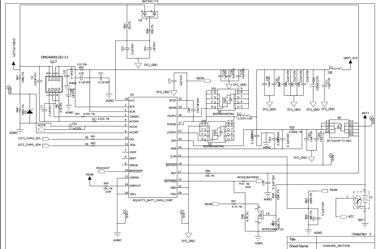
We are using  BQ24773 for battery charging .

Given below is the configuration of charger chip:

  1. Maximum battery charging current- 4A
  2. Maximum battery Voltage- 4.2V
  3. Switching frequency-600KHz
  4. Power adapter specs: 15VDC/3A

Average system load is 5.7A (max) , so in the scenario when both unit load and battery charging current is being drawn from the buck converter total output current requirement becomes 9.7A (approx.).

In this scenario the maximum temperature of different parts is as given below:

a) ACFET/RBFET (DMG4800LSD-13) : 96 ֯C 

b) High side MOSFET (BSZ0902NSATMA1): 85 ֯C

c) Low side MOSFET (BSZ0902NSATMA1): 94 ֯C

d) Inductor (SRP1038A-2R2M) : 98 ֯C

This temperature is measured when unit is working at 27 ֯C room temperature .

It will be really helpful if you can please provide your suggestions to reduce the temperature rise.

PCB is of 4 layers with size 50 mm x 28.5 mm and 2OZ copper thickness.


Schematic and pcb layout files are attached for your reference.

6457.PCB layout.pdf


Regards,

Mihir

  • Mihir,
    I think this post is a duplicated one of your another post below. The discussion is ongoing so I will close this one.
    e2e.ti.com/.../673076
    Regards,
    Eric
  • Hello Eric,


    This is different query related to PCB layout and design point of view. Kindly look into power dissipation and layout. Is there suggestion you would like to give? Please let me know if you want clarification regarding latest query.

    Regards,
    Mihir

  • First, do you have the FET loss estimation? For example, the ACFET, it should be easy because it doesn’t switch at normal operation. After you have the FET loss estimation, what the FET thermal impedance in the FET datashhet?

  • I am going to close this post since no new post in 3 days.
  • Please find below the information required by you:

    1. Measured Efficiency of Buck converter (charger)- 88.9%
    2. Average Load - 34W

    Prime contributors are :

    1. AC FET
    2. High side
    3. Low side Mosfet
    4. Inductor

    Please find attached data showing the practical values and the values obtained from theoretical calculations using 2 different methods i.e. as per the formulas given in the datasheet of BQ24773 and another is as per typical power dissipation method for buck converter.

    Given below is the summary of results:

    1. Calculation results as per datasheet

    Practical Values

    Theoretical Values

    Input Power

    38.266

    Input Power

    38.266

    Output Power

    33.99

    Calculated Pd

    1.62

    Efficiency

    0.888255893

    Output Power

    36.64348


    Efficiency

    0.957599


    1. Calculation results as per typical buck converter calculation

    Practical Values

    Theoretical Values


    Input Power

    38.266

    Input Power

    38.266

    Output Power

    33.99

    Calculated Pd

    3.12

    Efficiency

    0.888255893

    Output Power

    35.15


    Efficiency

    0.918565


    As given above there is a difference between the theoretically calculated values and practical values which probably is resulting  in temperature rise.

    Please suggest what could be done to reduce the power dissipation and in turn temperature rise.

  • Where do you measure the efficiency? For the datasheet, the input/output voltage were measured on the input/output sense resistor. So, it doesn't include the ACFET loss, BATFET loss and input cable or trace loss because customer can change the ACFET and have different layout.

    So, What is the voltage drop from your input voltage measurement point to ACP or SRN?
    Where is the hot spot on your board?

    Also, what FET do you use? There is a calculation tool to help you estimate the FET loss. www.ti.com/.../fetpwrcalc

    What inductor do you use? There is a calculation tool to help you estimate the inductor loss. www.vishay.com/.../
  • Hello Wang,

    Thanks for your response.  Please see below replies for your queries.

    1. Voltage drop between input voltage measurement point to ACP is 136.4mV.  

    2. Hot spot on the board: Common node of Drain (Low side FET), Inductor and Source (High side FET) and drain node of ACFET. Temperature of these component have already mentioned as below.

    a) ACFET/RBFET (DMG4800LSD-13) : 96 ֯C 

    b) High side MOSFET (BSZ0902NSATMA1): 85 ֯C

    c) Low side MOSFET (BSZ0902NSATMA1): 94 ֯C

    d) Inductor (SRP1038A-2R2M) : 98 ֯C

    We have two different calculation for FET losses.  (1) As per the formula given in datasheet of BQ24773 (2) As per typical MOSFET calculation in buck converter.

    (1) As per the formulas given in datasheet of BQ24773

    Power dissipation in charger circuit (W)
    P(ACFET/RBFET) 0.15
    P(HS) 0.36
    P(LS) 0.17
    P(L) 0.93
    Total Pd 1.62

    (2) As per typical MOSFET calculation in buck converter

    Power dissipation in charger circuit (W)
    P(ACFET/RBFET) 0.15
    P(HS) 1.55
    P(HS) 0.48
    P(L) 0.93
    Total Pd 3.12

    For the mentioned power dissipation as above for both cases what would be the temperature rise of component according to you?

    There is one more confusion regarding High/Low side MOSFET losses as listed below. Please answer the question.

    a) What is Ton and Toff in High side MOSFET switching loss? Is it rise/fall time or turn on/off delay time or summation of both rise/fall + turn on/off delay time during Gate turn on and turn off?  Part Number of HS/LS MOSFET: BSZ0902NSATMA1

    b) Why body diode losses and gate losses are ignored as only conduction loss is mentioned for Low side MOSFET in datasheet of BQ24773?

    c) What is your suggestion on Layout which is already posted in this ongoing query?

    Do let me know if any input you require.

    Regards,

    Mihir

  • Kindly correct the combined Pd of ACFET/RBFET is 0.4W instead of 0.15W.
  • a) What is Ton and Toff in High side MOSFET switching loss? Is it rise/fall time or turn on/off delay time or summation of both rise/fall + turn on/off delay time during Gate turn on and turn off? Part Number of HS/LS MOSFET: BSZ0902NSATMA1
    Ton and Toff should be rise/fall time. Not turn on/off dead time.

    b) Why body diode losses and gate losses are ignored as only conduction loss is mentioned for Low side MOSFET in datasheet of BQ24773?
    The low side FET's conduction loss is the dominate loss. At turn-on, the VDS is almost zero because of the inductor free wheel current passing the LOFET. At turn-off, the VDS is almost zero because of FET's Coss. But, the body diode losses should be added to total loss. The datasheet doesn't give several other loss calculation, such as the reverse recovery loss, gate drive loss... The datasheet mainly helps customer understand the charger function. No for optimize the converter efficiency. The datasheet efficiency curve was tested on an EVM.

    c) What is your suggestion on Layout which is already posted in this ongoing query?
    It is hard to review the layout with a pdf file. To get better thermal performance, please put power ground layer next to power FET's layer.
  • Hello Wang,

    Thanks for prompt reply.

    So as per your previous reply, considering rise time and fall time as ton and toff respectively, practically we are getting more ton and toff compared to datasheets of MOSFET and BQ24773. Kindly find attached captures of gate drive of HS and LS MOSFET.

    Practical values of ton, toff, t(dead on) and t(dead off) are mentioned as below.

    (1) ton = 16.70ns (Theoretical value as per MOSFET datasheet is 5.2nS)

    (2) toff = 13.62ns (Theoretical value as per MOSFET datasheet is 3.6nS) 

    (3) t(dead on) = 22.6ns (Theoretical value as per BQ24773 datasheet is 20nS)

    (4) t(dead off) = 55.8ns (Theoretical value as per BQ24773 datasheet is 20nS)

    NOTE: Waveform shown in Yellow is for GATE(HS) and Blue is for GATE(LS).


  • Would you find a local FAE to organize a webex meeting to discuss those detail?

    (1) ton = 16.70ns (Theoretical value as per MOSFET datasheet is 5.2nS)
    How do you get the calculate the 5.2ns?

    (2) toff = 13.62ns (Theoretical value as per MOSFET datasheet is 3.6nS)

    (3) t(dead on) = 22.6ns (Theoretical value as per BQ24773 datasheet is 20nS)

    (4) t(dead off) = 55.8ns (Theoretical value as per BQ24773 datasheet is 20nS)
    20ns is typical value. Also, we need to add the gate drive voltage from zero to Vth.

    NOTE: Waveform shown in Yellow is for GATE(HS) and Blue is for GATE(LS).
  • Hello Wang...!!

    Glad to hear you.. !!
    Can we talk after two days as I am on leave. Will get back to you as soon as possible.. Please make sure that this issue won't get closed till I get back to you. !

    And also will arrange meeting if require.. !

    Regards,
    Mihir
  • Sure. No problem. Wait for you come back.
  • Hello Wang,

    Hope you are fine..!

    Now coming back on the topic, we have taken 5.2ns as Ton time which is rise time of gate turn on as given in datasheet of MOSFET itself.

    Another thing is dead time is 20ns typically, it may be more than that practically.

    Can you please arrange a WebEx meeting with your FAE? or you can ask any of your local FAE to have a call with us? Please let me know the update regarding meeting.

    Waiting for your reply.

  • Would help me close this thread? And then, send an email to wang-li@ti.com to start an offline discussion.
  • Sure. What do u require to close this thread ?
  • Since we can email each other to discuss it offline, I am going to close this issue.
  • Hello Wang,
    Thanks for your support and help.You can close this issue here.
    Revert me on email asap.

    Regards,
    Mihir