This thread has been locked.

If you have a related question, please click the "Ask a related question" button in the top right corner. The newly created question will be automatically linked to this question.

uc2914 - SD pin

Hi all,

Would you mind if we ask uc2914?

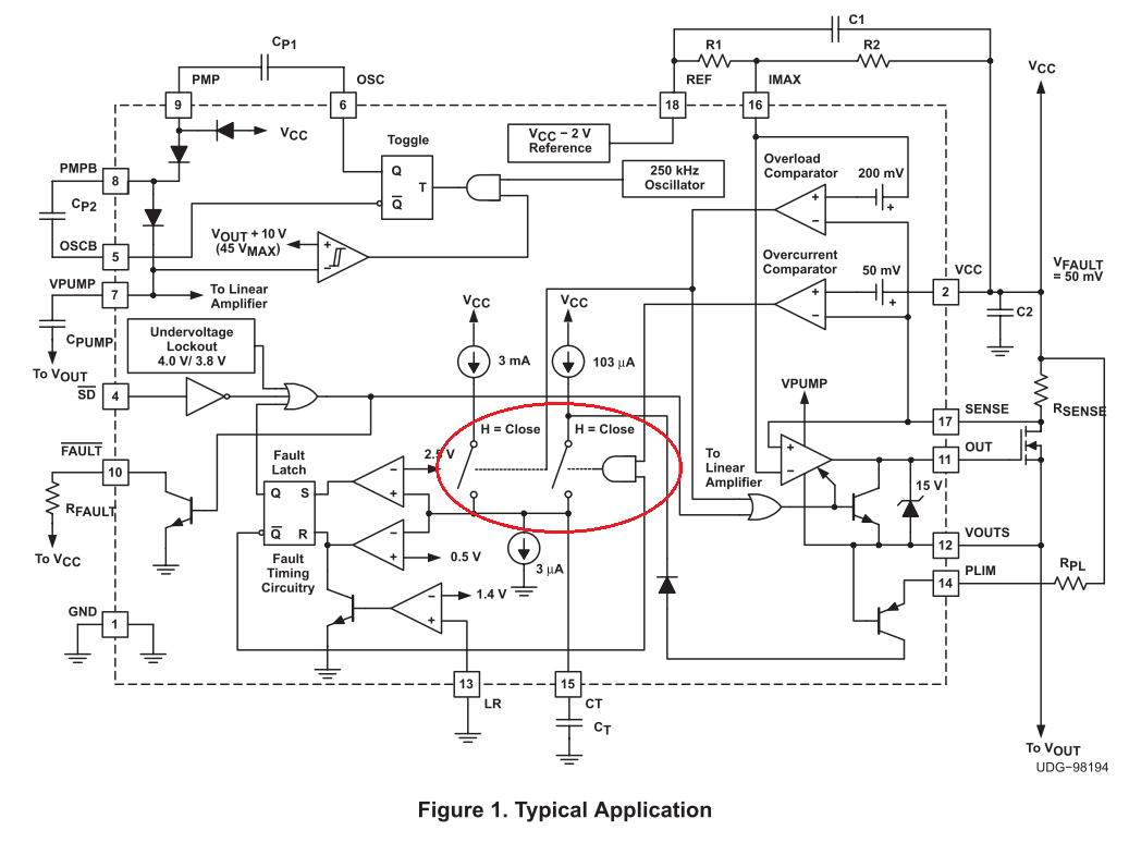
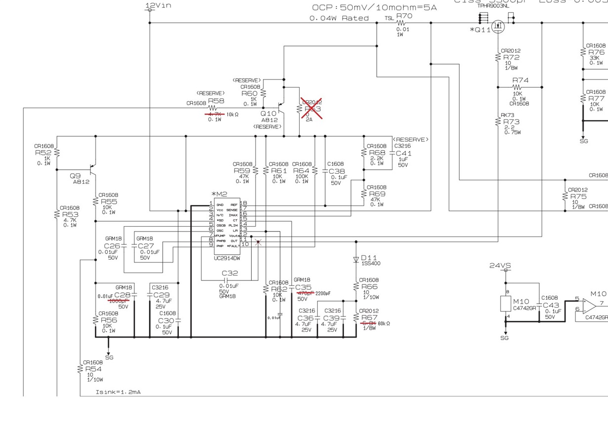
Please refer to following circuit.
4062.20141205_UC2914_circuit.pdf

We have some following questions;
<Q1><Q2>
3821.20141205_UC2914_Q1,Q2.pdf

<Q3>
0564.20141205_UC2914_Q3.pdf
Is this operation correct?

Kind regards,

Hirotaka Matsumoto

  • Hello,

    Below is my understanding based on the datasheet text:

    Q1: And then, after Overcurrent load, if SD pin set to low, the output didn't restart. Is this operation correct? The restart behavior is controlled by the LR pin (LR=high means latch off after fault and LR=low means retry after fault). If LR=high and a fault occurs then SD must be toggled from high-low-high to restart. Pulling SD=low anytime turns off the power switch.

    Q2: If SD pin set to low, is "Output Latch-off" released? Furthermore, LR pin is added 6V. The state of the device will remain OFF if SD is pulled low after a fault (while LR-=high). To restart, SD must go high again.

    Q3: There were chatterings at 4pin(SD), the voltage of CT increased, after that, the output voltage stoped. Abnormal and unpredictable operation can occur if there is noise on any hotswap enable (including UC2914 SD pin). Adding a small value capacitor can help filter unwanted SD pin noise.

  • Eric san,

    Thank you for your reply and your help!

    We 'd like to confirm followings;

    <Confrimation1>
    If LR=high and a fault occurs, until SD is toggled from high-low-high, it is not to restart.
    Is our recognition correct?

    <Confrimation1>
    We could not find your description "Abnormal and unpredictable operation".
    So, if you have much information about it, could you let us know?
    Because, we can not understand  on the block diagram why "Abnormal and unpredictable operation" occurs.

    Kind regards,

    Hirotaka Matsumoto

  • Confirmation #1: Yes, your recognition is correct.
    Confirmation #2: This is a general comment for any hotswap. The enable input pin (SD for UC2914) must be stable (without noise above/below the threshold) for predictable operation (ie, well above the ON threshold or well below the OFF threshold).
  • Eric san,Thank you for your reply!Kind regards,Hirotaka Matsumoto
  • Eric san,

    We appreciate your prompt response.
    Now we do need much your help. So could you let know us followings?

    <About Q1>
    We confirmed the condition of our customer's setting. 
    -LR pin remained High.
    -SD pin remained High(it was not toggled H L H).
    So, even though the setting is the latch-off of the output after a fault, after the output stopped, the output restart to operation 5V we mentioned before.

    <About Q2>
    "The state of the device will remain OFF if SD is pulled low after a fault (while LR-=high). To restart, SD must go high again."
    So, we got the method to restart,  but in this case, the fault latch off will be released or not?(it doesn't show on the datasheet)
    As the result of our customer's test,  the fault latch off was realeased and restarted.

    <About Q3>
    Thank you for your comment about SD-pin. 
    Of cource, we got that SD pin must be stable, there is no chattering, no noise.

    However, there are some various noise patterns(high frequnecy, low frequnecy).
    So, our cutomer asked us  how much of the speed on/off the device is allowed.(CT pin is charged? or not)
    If you have some information the deglitch time of SD pin, could you show us?

    Kind regards,

    Hirotaka Matsumoto

  • Eric san,

    We'd only like to mention about SD-pin ON/OFF chattering.
    If you have some advice, could you let know us?
    (Of cource, you don't have it, don't mind it)


    On the block diagram, according to SD on/off, we guess that CT is charged  momentarily.
    (If defalut is H-close.)
    So, on our customer's circuit, CT=2200pF, PLIM=48kohm.
    Compared with your reference circuit, the value of CT and PLIM is smaller(CT=0.1uF, PLIM=76.8kohm).
    So, it adversely affects to charge(charge and discharge time will be short.) .
    Is our recognition correct?


    And, if it is not effective to improve, we will try followings;

    <To prevent over voltage(under 2.5V) of CT pin>
    -Insert the XXMohm resistance between CT and GND(parallel resistance). 
    -Insert zener diode

    Kind regards,

    Hirotaka Matsumoto

  • Hello,
    Unfortunately, all the original team who designed this old part have left TI. I did not find an EVM either that I could use to help understand the operation of the UC2914 so for me the only available information is contained in the datasheet.
    In you customer's design, is it possible to consider a newer part for which TI could do a better job of supporting?
  • Eric san,Thank you for your reply and your help.
    Ok, we got your circumstance. Of cource, we accept your circumstance.
    However our customer already has(had) designed the board using this device.
    So, we have to support on the datasheet, then we told our customer that we can not get the detail of the device like as block diaglam.
    So, if you know Iout on the datasheet, please let know us the following.
    -How much of the value is the Iout(Pin11 Out)?
    It shows -2mA or not? We can not understand it.Kind regards,Hirotaka Matsumoto