This thread has been locked.

If you have a related question, please click the "Ask a related question" button in the top right corner. The newly created question will be automatically linked to this question.

66AK2H14: How DDR3 memory controller manage write accesses ?

Part Number: 66AK2H14

Hi,

I have made some test on writing directly data in DDR3A, in my test I do quite a few writes in DDR3A that is cached (through MAR registers).

For the following information I gave, I use DDR3 controller performance counter on DSP core0, and I measure R/W accesses.

For 1048576 Bytes input  uint32 data:

In no-optimized code (-o0), I have 262126 writes, that is for me logical (writing 4 Bytes by 4 Bytes).

In optimized code (-o3), only 36377 writes are counted by performance counter (I do not understand).

That makes sense ?

In my understanding of DDR3 controller documentation, the controller manage write command in its command FIFO and a scheduler send commands to SDRAM.
In a logic expectation, I was expecting for an input data, have a number of write acceses who correspound to: input data divided by sizeof(data), in my case 4 Bytes (uint32).

I put my test code in pseudo code:

table = @inDDR3A

test_size_bytes = 4;

do{

for(i=0; i <= test_size_bytes; i++){

table[i] = i;

}

test_size_bytes *=2;

}while (test_size_bytes < MAX_TEST_SIZE);

Regards,

François

  • Francois,

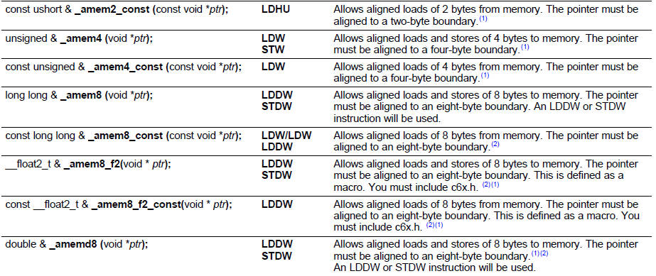
    You probably need to look at the resulting assembly to understand the reduced write cycles. Comparing your -o0 and -o3 performance the reduction in writes is by a factor of 7.2X times which makes me believe that the compiler is able to performed aligned reads from DDR or cache  for this data. C66x DSP can perform read or 4 bytes or 8 bytes using single instruction using LDW and LDDW while reading and STW STDW while writing  

    you can force the compiler to retain the assembly using -k option and compare the compiler output with -o0 and -o3 to see the software pipelining or optimization of the for loop.

    Regards,

    Rahul

  • Hi Rahul,

    I already used the -k option. My compilation option are :

    advice:performance=all --define=DEVICE_K2K -g --diag_warning=225 --diag_wrap=off --display_error_number --issue_remarks --debug_software_pipeline -k --gen_opt_info=2 --optimizer_interlist

    And I also read the assembly code I generated:

    For Optimized code (-o3) in DDR3 cached :

    $C$L5:    ; PIPED LOOP PROLOG
    ;          EXCLUSIVE CPU CYCLES: 2

               SPLOOP          1                 ;2 ; [A_L66] (P)
    ||         MV      .L2X    A4,B5             ; [B_L66]

    ;** --------------------------------------------------------------------------*
    $C$L6:    ; PIPED LOOP KERNEL
    ;          EXCLUSIVE CPU CYCLES: 1
        .dwpsn    file "../src/main.c",line 144,column 41,is_stmt,isa 0

               ADD     .L2     1,B4,B4           ; [B_L66] |144| (P) <0,0>  ^
    ||         STW     .D2T2   B4,*B5++(4)       ; [B_D64P] |146| (P) <0,0>  ^

               SPKERNEL        1,0               ; []
    ;** --------------------------------------------------------------------------*
    $C$L7:    ; PIPED LOOP EPILOG
    ;          EXCLUSIVE CPU CYCLES: 1
    ;**    -----------------------g4:
    ;**      -----------------------    return;
    ;** --------------------------------------------------------------------------*
    $C$L8:    
    ;          EXCLUSIVE CPU CYCLES: 6
        .dwpsn    file "../src/main.c",line 148,column 1,is_stmt,isa 0
    $C$DW$36    .dwtag  DW_TAG_TI_branch
        .dwattr $C$DW$36, DW_AT_low_pc(0x00)
        .dwattr $C$DW$36, DW_AT_TI_return

               RETNOP          B3,5              ; [] |148|
               ; BRANCH OCCURS {B3}              ; [] |148|
        .dwattr $C$DW$28, DW_AT_TI_end_file("../src/main.c")
        .dwattr $C$DW$28, DW_AT_TI_end_line(0x94)
        .dwattr $C$DW$28, DW_AT_TI_end_column(0x01)
        .dwendentry
        .dwendtag $C$DW$28

    For non-optimized code (-o0):

    ;** --------------------------------------------------------------------------*
    ;**   BEGIN LOOP $C$L26
    ;** --------------------------------------------------------------------------*
    $C$L26:    
    ;          EXCLUSIVE CPU CYCLES: 28
        .dwpsn    file "../src/main.c",line 146,column 9,is_stmt,isa 0
               LDW     .D2T2   *SP(12),B5        ; [B_D64P] |146|
               LDW     .D2T2   *SP(4),B6         ; [B_D64P] |146|
               LDW     .D2T2   *SP(12),B4        ; [B_D64P] |146|
               NOP             4                 ; [A_L66]
               STW     .D2T2   B4,*+B6[B5]       ; [B_D64P] |146|
        .dwpsn    file "../src/main.c",line 144,column 41,is_stmt,isa 0
               LDW     .D2T2   *SP(12),B4        ; [B_D64P] |144|
               NOP             4                 ; [A_L66]
               ADD     .L2     1,B4,B4           ; [B_L66] |144|
               STW     .D2T2   B4,*SP(12)        ; [B_D64P] |144|
        .dwpsn    file "../src/main.c",line 144,column 22,is_stmt,isa 0
               LDW     .D2T2   *SP(16),B4        ; [B_D64P] |144|
               LDW     .D2T2   *SP(12),B5        ; [B_D64P] |144|
               NOP             4                 ; [A_L66]
               CMPLTU  .L2     B5,B4,B0          ; [B_L66] |144|
       [ B0]   BNOP            $C$L26,5          ; [] |144|
               ; BRANCHCC OCCURS {$C$L26}        ; [] |144|
    ;** --------------------------------------------------------------------------*
        .dwpsn    file "../src/main.c",line 148,column 1,is_stmt,isa 0
    ;** --------------------------------------------------------------------------*
    $C$L27:    
    ;          EXCLUSIVE CPU CYCLES: 6
    $C$DW$96    .dwtag  DW_TAG_TI_branch
        .dwattr $C$DW$96, DW_AT_low_pc(0x00)
        .dwattr $C$DW$96, DW_AT_TI_return

               RETNOP          A0,4              ; [] |148|
               ADDAW   .D2     SP,4,SP           ; [B_D64P] |148|    
        .dwcfi    cfa_offset, 0
               ; BRANCH OCCURS {A0}              ; [] |148|
        .dwattr $C$DW$89, DW_AT_TI_end_file("../src/main.c")
        .dwattr $C$DW$89, DW_AT_TI_end_line(0x94)
        .dwattr $C$DW$89, DW_AT_TI_end_column(0x01)
        .dwendentry
        .dwendtag $C$DW$89

    I also red the documentation about CPU for instructions and pipelining and DDR3 controller documentation.

    But the are nothing on many bytes writing on only 1 write access.

    Do you think this is possible for example to write 30 bytes in one write access ?

    Regards,

    François

  • Francois,

    I have looped in colleagues from our compiler team to explain the change in behavior from -o0 to -o3 but based on the assembly,

    I can notice that the compiler has software pipelines the loop to allow multiple instructions to be executed during single cycle and has also managed to engage the Loop buffer using SPLOOP/SPKERNEL that reduces speculative loads/store operations.

    Regards,

    Rahul

  • Thanks for your answer,

    Ok for your analysis, I have the same understanding, but reduce speculative loads and store operations, means bigger bytes written in only one access ?

    Regards,

    François

  • For the source file that contains the test code, please follow the directions in the article How to Submit a Compiler Test Case.  That should allow me to comment on the performance difference between -o0 and -o3.  However, I doubt I will be able to shed light on why the DDR3 memory interface acts differently.

    Thanks and regards,

    -George

  • 6560.main.c
    /*
     * Author:  F. Poulain
     * Date:    05/06/2019
     *
     * The goal of this test is to see DDR3 behaviour in DSP one core writing.
     *
     */
    
    #include <memory.h>
    
    /* 1 MiB = 1024 KiB = 1048576  */
    #define DDR_SIZE_TO_TEST_MAX_BYTES    (0x100000)
    
    #define FLOAT_MB (1048576.0)
    
    /* */
    #define BUS_PRIORITY_MAX (0x0)
    
    /* */
    #define BUS_PRIORITY_MIN (0x7)
    
    #define MEM_CTRL_BASE_ADDR  (0x21010000)
    #define REG_SEL_CORE0   (0x00000000)
    #define REG_SEL_CORE1   (0x01000000)
    #define REG_SEL_CORE2   (0x02000000)
    #define REG_SEL_CORE3   (0x03000000)
    #define REG_SEL_CORE4   (0x04000000)
    #define REG_SEL_CORE5   (0x05000000)
    #define REG_SEL_CORE6   (0x06000000)
    #define REG_SEL_CORE7   (0x07000000)
    #define REG_SEL_LINUX   (0x08000000)
    
    /*
     *
     */
    void ddr_write_access(Uint32* p_tab, Uint32 size_bytes);
    Uint32 verif(Uint32* p_tab, Uint32 size_bytes);
    void init_cnt(void);
    
    /* */
    Uint32* ptab0 = NULL;
    
    int* cnt_1_addr;
    int* cnt_2_addr;
    
    
    float calculate_throughput(Uint32 size_bytes, UInt64 nb_cycles_elapsed)
    {
        float f32_speed_mb_per_sec = 0.0;
        double f64_speed_b_per_sec = 0.0;
        double f64_speed_mb_per_sec = 0.0;
    
        float execution_time_ns = 0.0;
    
        execution_time_ns = nb_cycles_elapsed * (1/1.2) ;
    
        f64_speed_b_per_sec = ( (double) 1000000000.0 * (double) size_bytes) / (double) execution_time_ns;
    
        f64_speed_mb_per_sec = f64_speed_b_per_sec / (double) FLOAT_MB;
    
        f32_speed_mb_per_sec = (float) (f64_speed_mb_per_sec);
    
        return f32_speed_mb_per_sec;
    }
    
    
    int main(void)
    {
        // memory initialization
        memory_init();
    
        // Variable used for the test
        Uint32 start_1=0;
        Uint32 start_2=0;
        Uint32 end_1=0;
        Uint32 end_2=0;
        Uint32 duration_1=0;
        Uint32 duration_2=0;
        Uint32 err=0;
    
        // Performance counter initialization
        init_cnt();
    
        // set priority
        Uint32 priority = BUS_PRIORITY_MIN;
        CSL_XMC_setMDMAPriority(priority);
    
        Uint32 core_id = 0;
    
        Uint32 size_to_test_bytes = 4;
    
        core_id = DNUM;
    
        // pointer in DDR3A
        ptab0 = (Uint32*) DDR_TEST_START_ADDR;
    
        if (core_id == 0)
        {
            /* Only Core 0 do the test */
    
            do
            {
                start_1 = *cnt_1_addr; start_2 = *cnt_2_addr;
                ddr_write_access(&ptab0[0], size_to_test_bytes);
                // Writeback last data in cache
                //CACHE_wbL1d(&ptab0[0], size_to_test_bytes, CACHE_WAIT); // commented because L1D is not write-allocate & cache is free at beginning.
                end_1 = *cnt_1_addr; end_2 = *cnt_2_addr;
    
                // Invalidate cache line (security to ensure empty cache)
                CACHE_invL1d(&ptab0[0], size_to_test_bytes, CACHE_WAIT);
    
                // Verification
                err = verif(&ptab0[0], size_to_test_bytes);
    
                if (err != 0)
                {
                    printf("Error: %d\n", err);
                }
    
                // reset all updated memory blocks in DDR3 memory
                memset(&ptab0[0], 0, size_to_test_bytes);
    
                // Writeback Invalidate cache (empty cache) due to verification
                CACHE_wbInvL1d(&ptab0[0], size_to_test_bytes, CACHE_WAIT);
    
                // Total read and write accesses by the DSP core #0
                duration_1 = end_1 - start_1; duration_2 = end_2 - start_2;
    
                printf("Data input: %dB, Read Acesses: %d, Write Acesses: %d\n", size_to_test_bytes, duration_1, duration_2);
    
                size_to_test_bytes *= 2;
            } while(size_to_test_bytes <= DDR_SIZE_TO_TEST_MAX_BYTES);
    
        }
    
        return 0;
    }
    
    void ddr_write_access(Uint32* p_tab, Uint32 size_bytes)
    {
        Uint32 i_word = 0;
        Uint32 nb_words = size_bytes / 4;
    
        for (i_word = 0; i_word < nb_words; i_word++)
        {
            p_tab[i_word] = i_word;
        }
    }
    
    void init_cnt(void)
    {
        // PERF_CNT_CFG
        int offset_cfg = 0x88;
        int *reg_cfg = (int*)(MEM_CTRL_BASE_ADDR + offset_cfg);
        *reg_cfg = 0x80038002; // CNT1: R, CNT2: W, DSP CORE0 MASTER ID
    
        // PERF_CNT_SEL
        int offset_sel = 0x8C;
        int *reg_sel = (int*)(MEM_CTRL_BASE_ADDR + offset_sel);
        *reg_sel = 0; // DSP CORE0 MASTER ID
    
        // PERF_CNT_1
        int offset_cnt_1 = 0x80;
        cnt_1_addr = (int*)(MEM_CTRL_BASE_ADDR + offset_cnt_1);
    
        // PERF_CNT_1
        int offset_cnt_2 = 0x84;
        cnt_2_addr = (int*)(MEM_CTRL_BASE_ADDR + offset_cnt_2);
    }
    
    Uint32 verif(Uint32* p_tab, Uint32 size_bytes)
    {
        Uint32 i_word = 0;
        Uint32 err = 0;
        Uint32 nb_words = size_bytes / 4;
    
        for (i_word = 0; i_word < nb_words; i_word++)
        {
            if (p_tab[i_word] != i_word)
                err++;
        }
    
        return err;
    }


    -mv6600 -O3 --include_path="D:/APP/TI_CCSV8/dsplib_c66x_3_4_0_2/packages/ti/dsplib" --include_path="D:/APP/TI_CCSV8/dsplib_c66x_3_4_0_2/packages" --include_path="D:/APP/TI_CCSV8/pdk_k2hk_4_0_12/packages/ti/csl" --include_path="D:/APP/TI_CCSV8/pdk_k2hk_4_0_12/packages" --include_path="D:/CoralieDev/projet/ddr3_perf_counter_w_access" --include_path="D:/CoralieDev/projet/ddr3_perf_counter_w_access/inc" --include_path="D:/APP/TI_CCSV8/ccsv8/tools/compiler/ti-cgt-c6000_8.2.5/include" --advice:performance=all --define=DEVICE_K2K -g --preproc_with_comment --preproc_with_compile --diag_warning=225 --diag_wrap=off --display_error_number --issue_remarks --debug_software_pipeline -k --gen_opt_info=2 --optimizer_interlist

    memory.c
    #include <memory.h>


    void memory_init (void)
    {
        int k=0;
        Uint8 pcx; // Reserved bit, do not touch
        Uint8 pfx; // prefetchability


        if (DDR_ACCESS == 1)
        {
            /*
             * MAR 128: DDR3 start @    : 0x8000 0000
             * MAR 255: DDR3 end @      : 0xFFFF FFFF
             *
             * DDR3 cacheabilty is enable on the entire DDR3 memory space.
             */
            for (k=128; k<=255; k++)
            {
                // Set PC at '1'
                CACHE_enableCaching(k);
                // Get the memory region information for MAR k
                CACHE_getMemRegionInfo (k, &pcx, &pfx);
                // prefetch, 0 disable, 1 enable
                pfx = 1;
                CACHE_setMemRegionInfo(k, pcx, pfx);
            }
        }
    
        else if (DDR_ACCESS == 0)
        {
            /*
             * MAR 128: DDR3 start @    : 0x8000 0000
             * MAR 255: DDR3 end @      : 0xFFFF FFFF
             *
             * DDR3 cacheability is disabled on the entire DDR3 memory space.
             */
            for (k=128; k<=255; k++)
            {
                // Set PC at '0'
                CACHE_disableCaching(k);
                // Get the memory region information for MAR k
                CACHE_getMemRegionInfo (k, &pcx, &pfx);
                // prefetch, 0 disable, 1 enable
                pfx = 1;
                CACHE_setMemRegionInfo(k, pcx, pfx);
            }
        }
    
        else
        {
            printf("MAR INITIALIZATION FAILED\n");
        }
    
        /* cache initialization */
        CACHE_setL2Size(CACHE_0KCACHE);
        CACHE_setL1DSize(CACHE_L1_32KCACHE);
        CACHE_setL1PSize(CACHE_L1_32KCACHE);
    
    }
    
    memory.hparameters.h

  • I do not find a way to send you the project folder, I sent you all files I use. Also do you need main.pp and memory.pp.

    I tried to follow your article, but if there any things missing, tell me.

    Regards,

    François

  • Because I don't have the preprocessed files, I am unable to compile exactly what you did.  However, I think I came close enough.  I can tell this function is the one you show the assembly code for in an earlier post ...

    void ddr_write_access(Uint32* p_tab, Uint32 size_bytes)
    {
        Uint32 i_word = 0;
        Uint32 nb_words = size_bytes / 4;
    
        for (i_word = 0; i_word < nb_words; i_word++)
        {
            p_tab[i_word] = i_word;
        }
    }

    Since it only depends on the type Uint32, I can compile it.  I used the build options you show in the previous post.  Except once I used -o3, and the other time I used -o0.  I compare the assembly code for those two builds.  So far as how the CPU accesses memory, there is no difference.  In each case, there is a loop around a single STW instruction.

    Thus, I am unable to explain why the system memory interface acts differently.

    Thanks and regards,

    -George  

  •  Hi George,

    This is the preprocessed files:

    main.pp.txt memory.pp.txt

    Otherwise for the proposed assembly code, it was compile with -oOff instead of -o0, sorry for the confusion. But  in  -oOff or -o0,  there is a difference in number of write accesses compare to -o3 option.

    Do you know if someone else could have an explaination or a way to explore ?

  • I look into write buffer for the moment,  it seems there is some write merging. But there is not a lot of information about that.

    Do you know anything about write buffer operation ?

    Regards,

    François

  • François,

    What is the question that you want answered? Compiler optimizations have nothing to do with DDR Controller operation.  Compiler optimization is all about stripping out superfluous CPU transactions and re-ordering CPU operations to minimize the time waiting for operands to reach the ALUs.

    Compiler optimization is separate from cache memory utilization.  Cache memory is provided as an intermediate storage for opcodes and/or data that may be needed again in the near-term.  The cache can also perform predictive pre-fetch that pulls in opcodes before the ALU needs them.

    Cache operations are also fully independent from DDR controller operation.  Optimized access to DDR is related to burst size and page boundaries.  All DDR accesses (writes and reads) by the K2H device will always be a full 8-strobe burst, even is the CPU only reads of writes a single byte.  Assuming your memory topology is 64 bits wide, the burst size is 64-bytes.  The most efficient DDR usage will always be in multiples of 64 bytes and be 64-byte address aligned.  This is why all cache fetches and line evicts are in multiples of 64 bytes and are 64-byte address aligned.  Optimal EDMA transfers to/from DDR will also follow this rule (or accesses from any other bus master).

    The DDR controller, independent of CPU activity, or that of any other bus master, will re-order transactions to optimize throughput.  Sequential read transactions or sequential write transactions with have higher throughput than interleaved read and write transactions.  Similarly, read and write transactions within a page are faster than sequential accesses that are to different pages.  The DDR controller can keep up to 8 pages open at a time to make this most efficient but again this is while managing transactions from all cores and all other bus masters.

    Tom

  • Hi,

    My question is why there is less write accesses at DDR3 controller when I use optimization for my code ?

    I have the same understanding as you on compiler optimizations, that's why I am surprised of results.

    In my case my memory topology is 32 bits, burst size of 32 bytes.

    I tried to align addresses, as you say, but nothing change.

    Also you mean banks by "pages" ?

    And also, just to let you know I have done some test in which I do sequencial accesses in a bank, the results I got are less efficient than sequencial writes through all banks. That's seems odd ?

  • Francois,

    In this context, banks and pages are not exactly the same.  The SDRAM Bank Activate command uses both the Bank Address bits and the Row Address bits.  This defines a page which is also referred to as an 'active row'.  See below text from Section 2.4.3 of the DDR3 Memory Controller User Guide (SPRUHN7):

    When the DDR3 memory controller issues an ACT command, a delay of tRCD is incurred before a read or
    write command is issued. Reads or writes to the currently active row and bank of memory can achieve
    much higher throughput than reads or writes to random areas because every time a new row is accessed,
    the ACT command must be issued and a delay of tRCD incurred.

    DDR throughput testing cannot be done from the CPU core.  The CPU memory accesses are far too slow and indeterminate.  You must use EDMA (actually more than one channel) to be able to control the bus transactions and DDR accesses sufficiently for this testing.  Any variations observed while changing compiler optimizations and cache configurations are performance variations due to those elements, not the DDR interface.

    Tom

  • Tom,

    Thanks, for your answer, in fact I asked you the question to be sure you are talking about pages. Besides in the optimized case there are less activates than the non-optimized case.

    But what I doesn't know, is the fact that I can't test DDR without using DMA. I will test using DMA and see what's going on.

    I'll get back to you if I have other questions about the subject using DMA, but I think you can closed this topic.

    Thank you very much for your help,

    Best Regards,

    François

  • François,

    Thanks for the confirmation.  I will close this thread.

    Tom