

Applications engineers tend to overlook printed circuit board (PCB) layout during circuit design. It is often the case that a circuit’s schematic is correct, but does not work, or perhaps works with reduced performance. In this post, I will show you how to properly lay out an operational amplifier (op amp) circuit PCB to ensure functionality, performance, and robustness.
An intern and I were recently working on a design together using the OPA191 op amp in a noninverting configuration with a gain of 2V/V, a 10kΩ load, and a supply voltage of +/-15V. Figure 1 shows the design schematic.
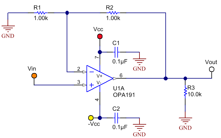
Figure 1: Schematic of the OPA191 in a noninverted configuration
I tasked the intern with laying out the PCB for this design. I gave him some general guidelines for laying out PCBs – keep traces as short as possible and keep components close together to minimize board space – and sent him on his way. How hard could it be? It’s just a few resistors and a couple of capacitors, right? Figure 2 shows the first attempt at the layout. The red lines are traces routed on the top layer and the blue lines are traces routed on the bottom layer.

Figure 2: First layout attempt
That’s when I realized that PCB layout isn’t as intuitive as I thought; I should have been a little bit more detailed with the guidelines. He did everything I recommended, keeping the traces relatively short and the components close together. The layout could be improved, however, to reduce PCB parasitic impedances and optimize performance.
The first improvement we made is moving R1 and R2 next to the inverting pin (pin 2) of the OPA191; this will help reduce stray capacitance on the inverting pin. The inverting pin of an op amp is a high-impedance node and is therefore “sensitive.” Long traces can act as antennas, which allow high-frequency noise to couple into the signal chain. PCB capacitance on the inverting pin can cause stability issues. Therefore, the connections on the inverting pin should be kept as small as possible.
Moving R1 and R2 next to pin 2 allows R3, the load resistor, to rotate 180 degrees, which then allows the decoupling capacitor, C1, to move even closer to the positive supply pin (pin 7) of the OPA191. It is extremely important to place decoupling capacitors as close to the supply pins as possible. Having long traces between the decoupling capacitor and the supply pin adds inductance on the supply pin, which can degrade performance.
Another improvement we made concerns the second decoupling capacitor, C2. The via connecting –VCC and C2 should never be put between the capacitor and the supply pin; it should be in a place where the supply voltage must pass through the capacitor before entering the supply pin of the device.
Figure 3 shows how to move each component and via to improve the layout.

Figure 3: Location of components for improved layout
Even after moving the components to new locations, it’s still possible to make additional improvements. You could make the traces as wide as possible to reduce the inductance of the trace – about the size of the pad to which the trace will connect. Another is to pour a ground plane on the top and bottom layer. This will create a solid, low-impedance path for return currents.
Figure 4 shows our final layout.

Figure 4: Final layout
The next time you are laying out a PCB, make sure to follow all of these layout practices:
- Make the connections to the inverting pin as short as possible.
- Place decoupling capacitors as close to the supply pins as possible.
- If using multiple decoupling capacitors, place the smallest decoupling capacitor closest to the supply pin.
- Do not place vias between decoupling capacitors and supply pins.
- Make traces as wide as possible.
- Do not route traces with 90-degree angles.
- Pour at least one solid ground plane.
- Do not sacrifice good layout to label a component with silkscreen.
Additional resources
- Learn more about stability in our TI Precision Labs – Op Amps training series on stability.
- Read about issues related to decoupling capacitors in amplifier expert Art Kay’s blog, “The decoupling capacitor … is it really necessary?”
- Find commonly used analog design formulas in our wildly popular and free Analog Engineer’s Pocket Reference e-book (myTI login required).
- Read more blogs about precision amplifiers.
- Learn about TI’s entire portfolio of amplifier ICs and find technical resources.
-

Tim Claycomb
-
Cancel
-
Up
0
Down
-
-
Reply
-
More
-
Cancel
Comment-

Tim Claycomb
-
Cancel
-
Up
0
Down
-
-
Reply
-
More
-
Cancel
Children