This thread has been locked.

If you have a related question, please click the "Ask a related question" button in the top right corner. The newly created question will be automatically linked to this question.

VCA2612: Where do i have to place the capacitor for compensation when using active feedback

Part Number: VCA2612

Hello,

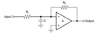
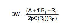
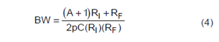
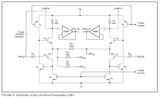
in a hardware design i am using the VCA2612 with two differential input signals. The VCA2612 provides a compensation when using active Feedback. The value for the capacitor is calculated with Equation 4 in the datasheet (see below).

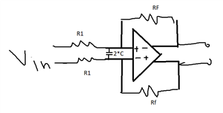
The Question for me is where i have to place it for both channels (A and B)?

Is it between pin 10 (COMP1A) and 11 (COMP2A) for channel A and between pin 27 (COMP1B) and pin 26 (COMP2B) for channel B?

Or should I use Figure 4 as a guide and place the capacitor between pin 11 (COMP2A) and pin 16 (LNP_IN_PA) for the positive input and between pin 10 (COMP1A) and pin 12 (LNP_IN_NA) for the negative input of channel A?

In this case there is to place the capacitor for Channel B between pin 26 (COMP2B) and pin 21 (LNP_IN_PB) for the positve input and between pin 27 (COMP1B) and pin 25 (LNB_IN_NB) for the negative input, right?

Thank you in advance.

  • Hi,

    Datasheet recommends to place compensation capacitor between Input terminal and Ground whenever active termination is used. 

    If your using differential input, instead you can place compensation capacitor between LNP_IN_P and LNP_IN_N and enable active termination. This cap will provide enough stability for active termination loop and also, gives you a LPF corner based on below eq-

    Circuit below,

    Regards,

    Kalyan

  • Hi,

    thank you for your reply. If i place the compensation capacitor between LNP_IN_P and LNP_IN_N as shown in the picture above, i come to the question for the meaning of the connections COMP1 and COMP2?

    Thank you in advance.

  • Hi Richard,

    The circuit shared previously would work well when you plan to use both active termination feature (Rf) and  also if you want to control the bandwidth. I shared that circuit because it satisfies the BW specified in the eq(4) which you shared. If you don't want to use feedback RF, as you already mentioned, you can connect compensation capacitors between LNP_IN_P and COMP2A, LNP_IN_N and COMP1A. In this case BW can be computed as below,

    BW = 1/(2pC(A+1)R1)

  • Hi Kalyan,

    and if i neither use the active feedback nor place capacitors between LNP_IN_P and COMP2A, LNP_IN_N and COMP1A, the bandwidth of the VCA2612 remains unchanged.

    Thank you alot, then i will use the first circuit variant with the active feedback.

    Regards, Richard