- Ask a related questionWhat is a related question?A related question is a question created from another question. When the related question is created, it will be automatically linked to the original question.
Hi Team,
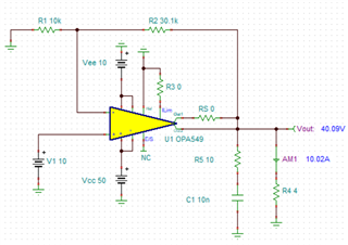
![]()
The image above is about my application. Amplify the input by ratio 4, i.e. if input = 10V, then output = 40V. Besides, the input is a square wave.
And here I did a short on output, which made the output short to GND directly and then disconnected the output immediately. As the setting of RCL = 0Ohms, the current limit should be at 10A.
But after the operation, I found that the output cannot work as expected (before the operation it works well). I connected the output to a DC-DC EVM input terminal but cannot get the right waveform.
I would like to know if it is OK to short output to GND directly? Does the chip has been damaged?
Thanks.
Bing