- Ask a related questionWhat is a related question?A related question is a question created from another question. When the related question is created, it will be automatically linked to the original question.
Hi all,
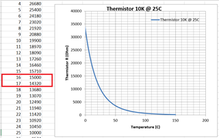
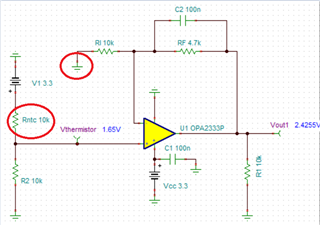
We are working on a design that needs to measure temperature at two points. We are using NTC thermistors (resistance at 25C is 10K) for it. In order to interface the NTC outputs with a MCU , we
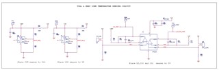
have selected OPA333. The schematic with the NTC thermistors is attached. TI's reference design Temperature sensing with NTC circuit is referenced for our design.in this reference design the featured
product is TLV9002; but OPA333 can use as alternate(also in the reference design).
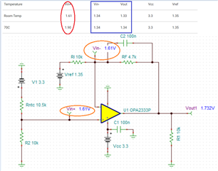
The design is such that to get a output swing of 0.05 V to 3.25V.(-10 to 60 degree.C)
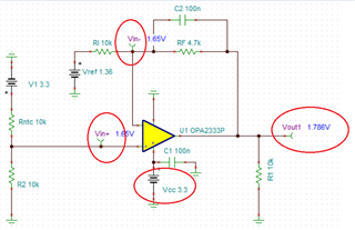
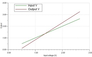
When the temperature across the NTC is varied , we can observe the change in voltage at the terminal of the Op amp (non-inverting terminal. The input swing is between 0.5 V to 2.65 V. But at the output ,
we could not get the expected swing . At lower temperature, the output seems clamped at 1.35 V ( the reference voltage) and for higher temperature the output just rises to 1.5V. The reference voltage is
stable at 1.35V.
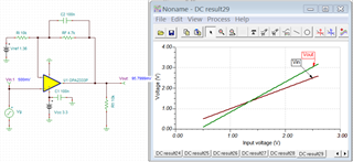
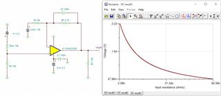
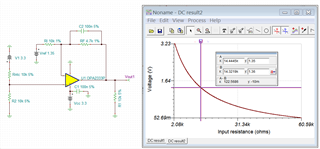
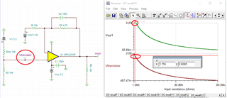
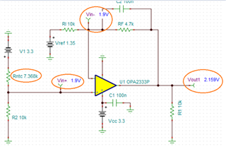
We have done the simulation in TINA with
and we have got the expected gain (1.5) and output. the simulated circuit and DC transfer characteristics is given below.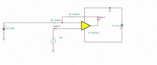
.
Request to help us understanding the cause for this issue and a solution for it.
I am also attaching the detailed design document with my simulation results and reference design.
With Regards
Adarsh
NTC thermistor with OPA333 design.pdfNTC temp_using TLV9002.pdf