This thread has been locked.

If you have a related question, please click the "Ask a related question" button in the top right corner. The newly created question will be automatically linked to this question.

TLV6710: OUTB oscillating. is this normal?

Part Number: TLV6710

Hi,

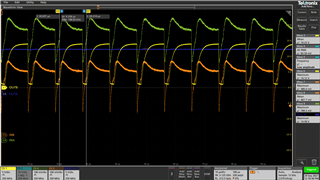
I am reaching out to you in regards to the TI TLV6710DDCT window comparator. I was running some tests on it today so the comparator monitors the same voltage as VDD. When doing this, OUTA acted as planned and had no issues, but OUTB seemed to have a 1 V period where it was oscillating between 0 and the voltage it was receiving. So, between 14.2 V and 15.2 V the comparator would not shut off completely. I tested this with two parts and saw it in both cases. I am wondering if this is something that’s happened before or if it is the typical behavior in regards to the voltage gap. If you have any information on that it would be helpful.

Thanks,

Kevin 

  • Hi Kevin,

    Can you provide a full schematic and also a scope shot if possible? What is the power supply source and voltage?

    What is the output pull-up resistor value?

    My first guess is that there is inadequate supply bypassing. Since it is an open collector output, and you are monitoring the same voltage that is being used for the pull-up, the output going low could be drawing down the supply, causing a supply glitch that feeds-back.. Also see figure 26 on page 18, which hints at cleaning up the supply.

    And make sure the input voltages on either of the input pins do not exceed 1.7V when you are up above 14V.

  • Hi Paul,

    thanks for picking up this support ticket. please see below for customer feedback

    I ran some more tests on it today implementing your recommended RC filter in them. Unfortunately, the problem persists. Once we reach a value around 14.2 V the voltage at INA, INB, and OUTB begin to oscillate together ( you can see this in the screenshot of the scope attached ) which continues until around 15.6 V. INA and INB only begin to oscillate when OUTB oscillates. OUTA outputs a clean signal and never oscillates, operates as planned. We are assuming there is some feedback somewhere in the component giving us this oscillating output.


    The schematic is built the exact same as Fig. 22 on Page 14 with the following resistor values.

    R1: 1M (From VDD to INA)

    R2: 22k (From INA to INB)

    R3: 30k (From INB to GND)

    The output pull up resistors are 100k.

    In the screen capture see left hand side for Signal labels. VDD = 14.6 V

    We are using a lab power supply to test the circuit running at 5 mA and changing the voltage from 5 V to 17 V to ensure the component is working correctly.


    Let me know if I can answer anymore questions for you to help you get a better understanding.

    Thanks,

    Kevin 

  • Hi Kevin,

    Try placing a 10nF cap from INA to GND, to bypass the input signal (provide low AC impedance).

    Are the output traces near the inputs? The outputs are swinging 15V and can kick quite a signal back into the relatively high impedance inputs through capacitive coupling if the I/O traces are near each other. Is this on a PCB or breadboard?

  • thanks Paul. it is resolved. it was tested on a breakout board!