This thread has been locked.

If you have a related question, please click the "Ask a related question" button in the top right corner. The newly created question will be automatically linked to this question.

OPA2846: Noise in pulse shaper with wide bandwith (MPPC signal)

Part Number: OPA2846
Other Parts Discussed in Thread: OPA695, OPA855, LMH6629, OPA847, OPA846

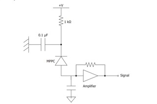
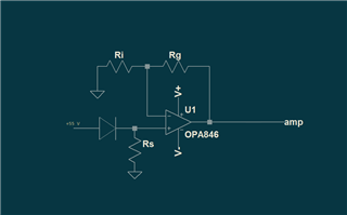
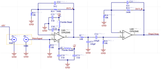
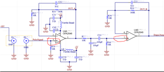
I am using an MPPC with voltage amplification with the circuit shown below. The circuit is a pulse shaper to count photons, it counts with 4 amplifing stages (OPA 2846) and a comparator (LT1719) at the end.

The MPPC is powered with +55 V through a coaxial cable and pulse signal is collected by another coaxial cable.

MPPC manufacturer told me that the ideal bandwith is up to 300 MHz. The problem is that with this configuration i´m having too much gain and a wide bandwith.

I´ve made different boards and in all of them I´ve had different issues.

  • First I started with 2 different boards both of 2 layer and struggled with the configuration to reduce noise until I have a good signal at the end. For both boards i got two different configurations.
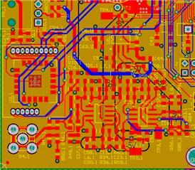
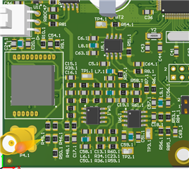
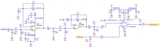
  • Then i moved to a 4 layer board(1:-Signal,2:-Ground,3:-Power(+5V,-5V,3.3V),4:-Signal) to reduce noise effect. I copied the confiuration used in the 2 layer board but again i got an oscilation near 100 MHz. Finally i removed this oscilation adding a 10 ohm and 100 pF at the output of each opAmp to compensate the peak gain, reducing AB.

As you can see i keept the gains of the stages near 10, the resistors seen by the opAmp at V+ and V- are of 50 ohms to keep them matched, the 1kohm resistor seen by the LT1719 comparator are also matched. I keep the traces as small as posible and try to avoid jumping from layer 1(signal) to layer 4(also signal).

I want to know if there is a PCB routing recomendation and opAmp stages configuration that could improve the SNR and avoid unwanted oscilations.

  • Morning Nacho, 

    Kind of an ambitious level of gain bandwidth, but it looks pretty good to me. 

    One small point to try if possible is to insert a 10ohm at each V+ node after the last shunt element, where the circles are here - the input stages are touchy to reactive source Z at higher F. Not your issue likely, but good practice, 

    Also, when you are cascadeing such high gain bandwidth, I suggest a pi supply filter from the last stage to the first - as I suggested in this long ago app note, starting on page 10. This one is about CFA mistakes, but the cascaded high gain bandwidth design is applicable with the OPA2846 as well, 

    https://www.ti.com/lit/an/snoa367c/snoa367c.pdf

  • And incidentally, when you do these cascaded stages, once you get past the 1st low noise stage, the subsequent stages do not degrade SNR much. Starting from scratch, I would be using an OPA855 1st stage (or LMH6629, or OPA847) followed by OPA695's perhaps. Also, if the overall path is AC coupled as you show, you could eliminate the blocking caps by wrapping a DC correction servo around the entire forward path. 

  • Thanks for the answer Michael. I will keep in mind all the tips you gave me. 

    I´ve noticed that transimpedance configurations appears in the most of the datasheets of the OpAmps you suggest. I know that with high capacitance(~1500 pF is my case) the transimpedance configuration doesn´t suite for the AB that the MPPC manufacturer told me(up to 300 MHZ). Is this OK or should i try with this config?

  • Hello Nacho,

      For PCB recommendations, it is best to follow the layout guidelines that are usually found at the end of the device's datasheet. Specifically for high frequency applications, it is best to cut out a small section of the power and ground planes under the signal input and output pins of the amplifier. This will minimize parasitic capacitance from these pins to ground. Also, try to keep the MPPC as close to the input of the amplifier as possible. Also for the filtering at the power supplies, the capacitors will be later populated? Would you be able to share a snippet/image of your layout for further recommendations? 

      1500pF is a lot of input capacitance. I thought MPPCs have lower capacitance. Is the 55V bias to the photodetector at the higher end of the capacitance curves for the photo detector? With a high input capacitance, it will be difficult to achieve 300MHz and a high gain in the first stage.

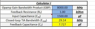
      (calculator can be found here)

    Thank you,

    Sima

  • Thanks Sima,

    About the filtering power supply, at this moment, I have a 6,8 uF then the ferrite and then a 1nF and 10 pF.

    In this design the MPPC is connected by 2 coaxial cables and i think this would be difficult to change due to the optical design.

    Idealy most MPPCs have lower capacitance but in this case i´m using the S13360-6075 wich has a big photosensitive area as you can see in the datasheet.(https://www.hamamatsu.com/resources/pdf/ssd/s13360_series_kapd1052e.pdf). In an MPPC the larger the photosensitive area is the bigger capacitance the MPPC will have.

    Here a image form my layout.

    PD. sorry for my bad english

  • Hello Nacho,

      Thank you for the additional information. Ah, I see now, thank you for the explanation on MPPCs!

      The PCB is very organized; these are minor suggestions, but some components could be placed closer to the pins of the amplifiers. Also, we usually suggest widening the trace to the pads of the decoupling capacitors and placing a few GND vias around that section. Here is a PowerPoint explaining in depth on high-speed PCB layout techniques

       Sorry, I missed this earlier, but the MPPC is a current output detector. Is there an amplifier stage before the OPA2846? Otherwise, it would need to be connected directly to the inverting input of the amplifier for a transimpedance application. Also, since, there will be a coaxial cable between the photo detector and the TIA, it is recommended to include a DNP input cap to ground very close to the inverting input of the TIA. This might be needed if there is too much inductance isolating the capacitance of the MPPC from the amplifier system, since it looks like you would need to place a relatively large feedback capacitor.

    (Edit: forgot to include feedback cap in parallel to feedback resistor)

      And, no worries, your English is very good.

    Thank you,
    Sima 

  • Hi Sima,

    Thanks for your recommendations and the powerpoint.

    Actually, there is no amplification stage before opa846. When a photon avalanche occurs, the current flows to the shunt resistor (Rs).

    Here i leave a basic photo of how it is at the moment(withouth inlcudiong the coaxial cables)


    Here I leave a basic photo of how it is at the moment (not including the coaxial cables).

    i will consider the DNP capacitor for future designs.

    Thank you,
    Nacho
  • Hello Nacho,

      The reference photo was very helpful. Looks like you are using the MPPC not in in the usual transimpedance configuration. This technically would work, but we would not recommend this solution because this changes the loading properties on the photodiode. In the transimpedance (inverting) configuration, the source essentially sees a near zero input impedance. In this non-inverting voltage feedback case, the source sees RS which will affect the common-mode input voltage to the amplifier with variations to the resistor. Also, this will contribute more noise and offsets that follow high input impedance solutions due to the bias current of the amplifier. A FET input amplifier would be required here, so you would not be able to gain the benefits of the low input offset voltage of a bipolar with only needing a very low feedback resistor.

    Thank you,

    Sima