This thread has been locked.
If you have a related question, please click the "Ask a related question" button in the top right corner. The newly created question will be automatically linked to this question.
Hello,
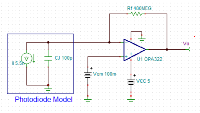
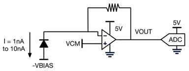
I am designing the following basic photodiode current sensing circuit. I am holding my common mode voltage at 100mV and my resistance is 480MOhm. My goal is to be able to operate with a 10kHz input signal. The photodiode has a Cj of 100pF.
To calculate my transfer function: Vout = Ipd*Rf + Vcm = I * 480Mohms + 100mV
Using this transfer function I was able to calculate the minimum output voltage at 1nA to be 580mV. How is it possible that my ouput voltage is able to go lower than this minimum value of 580mV?
What are some additional design considerations when choosing an op amp for these types of applications?
Hey Lucas,
We have a cookbook circuit that discusses key design notes, please see the Photodiode Amplifier Circuit
As for your question the voltage output swing is from 0.1V to 4.9V (based on 5V V+) OPA322 ds:
Replacing with the Imax given (10nA), R1=480MΩ
Therefore the simulation you have attached is correct, Vo lower output swing ~100mV.
All the best,
Carolina
Thank you for the collateral, I have been using that for this project. I guess my question is more about the output voltage equation I solved for:
Vout = Ipd*Rf + Vcm = I * 480Mohms + 100mV
Is this correct? If so, why doesn't it hold true for the minimum current of 1nA?
Best regards,
Lucas Pucheta
Hello Lucas,
This does hold true at 1nA.
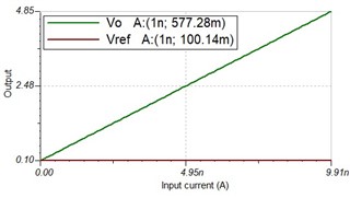
Please see the DC analysis below, at 1nA the output is close to 580nA:
Did you see the 1 MHz, Single-Supply, Photodiode Amplifier Reference Design? It is a little bit more detailed than the cookbook alone.
All the best,
Carolina
Thank you!!!
So to calculate my DC error at 1nA , can I use the following equation?
Calculated: Vout = 580mV
Simulated: Vout = 577.14mV
DC Error: (1-577.14mV/580mV)∗100 = .493%
Best regards,
Lucas Pucheta
Lucas,
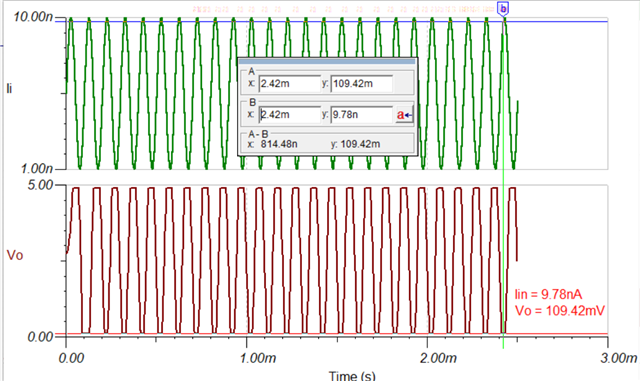
Your signal appears to be clipping. Clipping adds distortion and a time delay. Reduce signal or gain. Also get waveform for IN- node. It's shape should be same as output except smaller and lead by 90 degrees. If it distorts , try reducing amplitude or gain.
Ron,
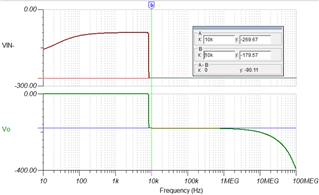
You were right about the VIN- node leading by 90degrees, is due to the dominant pole internal to the op amp? The clipping in the output voltage is clear in the transient analysis. I have to use this photodiode input current signal so maybe I can reduce my gain. Could I just choose an amp with a lower open loop gain as opposed to changing the feedback resistor?
I have added my TINA-TI file to the post.
Best regards,
Lucas Pucheta
Lucas,
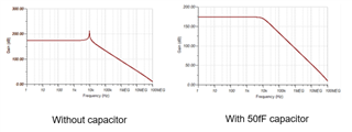
The model has a resonance (gain peak near 9kHz) , adding even 50 femto farads across the 480M ohm resistor fixes that issue.
There will be some natural capacitance in a real resistor and the PCB footprint.
At 10 kHz there is not enough op amp gain to preserve the DC operating point.
Hello Ron,
Could you explain your statement regarding not having enough gain at 10kHz to preserve DC operating point?
Wouldn't the system have more gain at 10kHz if I don't use a feedback cap?
Best regards,
Lucas Pucheta
Lucas,
The system (everything in it) is asking for more gain (without cap). The op amp has the same gain ( [op amp output] / [op amp input] ) in both configurations. For best performance the op amp should have significantly more gain than the whole system requests. The results with the chosen op amp and results with a perfect ideal op amp should be close to the same. Otherwise the system will be too sensitive to variability in op amp sample to sample performance.