- Ask a related questionWhat is a related question?A related question is a question created from another question. When the related question is created, it will be automatically linked to the original question.
This thread has been locked.
If you have a related question, please click the "Ask a related question" button in the top right corner. The newly created question will be automatically linked to this question.
Like commented in title, I did a schematic to amplify the difference between in+ and in-.
So when in+ is equal in-, I hoped that output would be the value of reference. But that doesn't happen.
In this case, I hoped that the output would be 1V, but I read 200mV, when in+ equal in-.
Schematic:
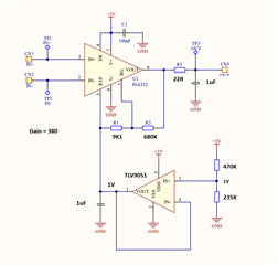
Infos:
Vcm (common mode): 1.5V
Gain: 380
VREF: 1V
VCC: 3V
Hi Marcus,
You are correct that you should have measured 1.0V + Vos*gains, where the circuit gain = 378.6V/V.
Everything looks good from the attached schematic. Could you check your the input and make sure that you have bias current return path to ground at the input?
Enclosed is the simulation for your reference.
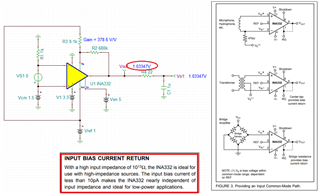
INA332 Vout Issues 12092021.TSC
Best,
Raymond
Thanks for the reply and for the attention.
We are using Wheatstone Bridge and the 4 resistors have a value of 10KOhms.
Hi Marcus,
Please remove the 1uf capacitor from TLV9051 and place it to the other side across 235kohm resistor. Op amp does not like to drive capacitor because it creates additional pole in the feedback loop. Please let me know if this fixes it.
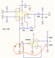
This is your INA332 configuration:
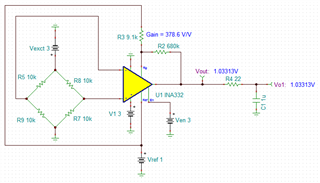
Best,
Raymond
I marked it as "resolved" wrongly, I made the change and the output continued with the same behavior, I will try to measure the noise/gain to try to help with some new solution. Soon I bring news
Hi Marcus,
Your circuit should measure the following voltage from your previous description. Vref should measure at 1.0V and Vcm are configured at 1.5Vdc. The transfer function at the output is Vout = Gains*(Vin+ - Vin-) + Vref, where gains = 378.6 V/V and (Vin+ - Vin-) = 0 without input stimulus or Wheatstone bridge is balanced.
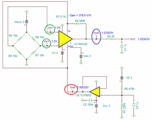
Enclosed is the Tina-TI simulation. If the Vout is still measured at 200mV under the above condition, please check your wiring connections. If you have additional questions, please let me know.
INA332 Vout Issues 12102021.TSC
Best,
Raymond
Fiz todas essas medições e tudo condiz com a sua imagem, com exceção da saída, que ao invés de ser 1V, é 200mV...
Very strange.
Hi Marcus,
Did you use TLV9052 part with thermal pad? The thermal pad is required to connect to the most negative power rail or V- in a design. For a single supply rail, the thermal pad is required to be connected to ground.
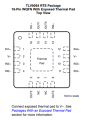
If you have other questions, please let me know.
Best,
Raymond
We are not using this encapsulation, we are using MSOP-8...
I'm finding it very strange not having the result of your simulation, the values and connections are all right.
In another test, we take the TLV and put a variable voltage source on the reference pin, and the problem remains.
Hi Marcus,
Sorry to hear that you are still having the issue.
Could you replace the existing INA332 part on the PCB? If all the pins and feedback are connected properly, I do not see why it should have the issue, unless the IC is damaged for some unknown reasons.
Below is the Vcm and Vout linear relationship, and your system configuration is operating within the boundary.
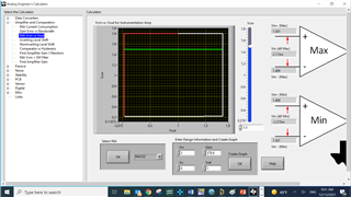
Best,
Raymond
Hi Marcus,
With the balanced Wheatstone bridge and Vcm = 1.5V, what is the voltage measured at the node marked in green? When the differential input voltage is 0V, the Vout = Vref = node marked in green circle. Please disconnect R7 resistor when you perform the measurement.
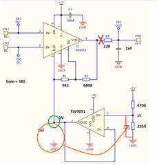
does it make sense to send the assembled board for analysis?
It will be a quicker to replace the existing INA332 part and see the result. I assumed that you have checked all the PCB traces (no layout mistakes).
BTW, I have assumed that INA332 part is purchased from TI authorized distributors. If it is not, your guess is as good as mine. To send the board for analysis, it will take a lot longer. Sure you may do that, but there must be a reason why the circuit is not working as it should.
Best,
Raymond
I set up 3 boards and each board has a different behavior, one output I measure 200mV, the other 500mV... I'm going to do this test you suggested and I'll tell you the result. Is it to disconnect the R7 or R3?
Hi Marcus,
Please remove R3 or 22Ω resistor, which it will disconnect INA332's Vout from ADC.
If all 3 boards are configured the same, the INA332's Vout should measure the same. Please short the differential input, (Vin+ - Vin-) = 0V, measure the voltage at the output of TLV9051 and red "X" node after 22Ω is removed.
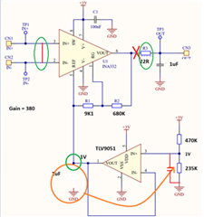
Best,
Raymond
I did what you recommended and the problem continued...
Even working with a wrong output, it's working for my application, but I'm having doubts about this operation, I'm finding it quite strange.
Can we send a board for review? I don't mind if it takes a few days, I just want to understand the problem.
Hi Marcus,
Can we send a board for review?
You may send us the Gerber file and I will review the layout. Our facility is winding down toward the end of the week and ready for the upcoming holidays.
Can you perform the following tests of the circuit?
1. Remove R1 resistor, and short R2 resistor --> this will configure the gains of the circuit at 5V/V. If you short the INA332's input or Vin+ = Vin- = Vcm, Vout should be measured at 1V or Vref node. If Vout is still measuring at approx. 200mV-500mV, please remove INA332 instrumentation amplifier and replace it with a fresh one.
2. I assumed that you purchased these parts from TI authorized distributors. And these parts have not been damaged such as over temperature (during fabrication and/or assembly or similar), electrical over stress etc.. It is odd that all three PCBs have shown similar issues.
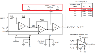
Best,
Raymond