This thread has been locked.

If you have a related question, please click the "Ask a related question" button in the top right corner. The newly created question will be automatically linked to this question.

OPA838: RF – Small Signal Low Noise Amplification and Demodulation

Part Number: OPA838
Other Parts Discussed in Thread: OPA820, , OPA684, OPA683, TLV3501, LM2596, LM2674, TLE2426, LM27762, TINA-TI, LMV7219

Due to the requirements of the application, most notably temperature and vibration, I have been unable to find suitable RF LNA or OOK demodulation packages as off-the-shelf products.  Therefore I am designing a receiver specifically for this application.  I encountering several problems in the design of this receiver. 

Key Questions:

  • Why the distorted output from the high Q band-pass filter?
  • Why does the third amplifier stage not amplify in “realistic” simulations using Boyle model?
  • Why do the amplifiers not manage large signals very well?

The rest of this document is an effort to give a detailed description the shortcomings of this receiver design as it relates to questions 1-3.


APPLICATION

I am building an RF receiver to receive a transmitted serial data stream.  The receiver can be very close to the transmitter, which results in a very strong signal being received.  The receiver must be able to demodulate a very large signal (as large as +24 dBm).  The receiver can also be very far from the transmitter, which results in a very weak signal being received.  The receiver must be able to demodulate a very small signal (as small as -56 dBm). 

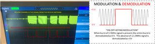
The RF transmitter is transmitting a 1.5 MHz carrier wave.  The transmitter modulates the carrier wave using On-Off Keying at a frequency of 133 KHz to encode the serial data stream message.  A dominant bit is transmitted as a 7.5us burst of 1.5 MHz carrier wave.  A recessive bit is transmitted when the carrier wave is switched off.


  RECEIVER DESIGN REQUIREMENTS

  • Environment
    • 125°C Maximum Operating Temperature
  • Receive RF Signal From Antenna
    • On-Off Keying (OOK) modulation
    • Carrier Frequency = 1.5 MHz
    • Message Frequency = 133 KHz
  • Small Signal Amplification
    • V_IN_MIN = 0.001 Vpp (-56.02 dBm)
    • V_OUT_MIN = 2 Vrms (19.03 dBm)
    • Total Gain Required >= 75 dBm
    • Amplification Factor = ~5,500 V/V
  • Large Signal Attenuation
    • Max Attenuation Required >= -1.43 dBm
    • AMPLIFICATION FACTOR = ~5,500 V/V
    • V_IN_MAX = 10 Vpp (23.98 dBm)
    • V_OUT_MAX = 3 Vrms (22.55 dBm)
  • FILTER
    • Isolate carrier frequency in very noisy environment
    • Implement high Q factor band pass filter (Q>=10)
  • DEMODULATION
    • Implement envelope detector
    • INPUT MODULATION = ON OFF KEYING (OOK)
    • CARRIER FREQUENCY = 1.5 MHz
    • MESSAGE FREQUENCY = 133 KHz
    • DOMINANT BIT = SIN WAVE
    • RECESSIVE BIT = NO SIN WAVE
    • OUTPUT MODULATION = SERIAL DIGITAL
    • DOMINANT BIT = 0 VOLT
    • RECESSIVE BIT = 5 VOLT
    • OUTPUT RAMP TIME <= 0.5uS
    • OUTPUT FALL TIME <= 1.5 uS
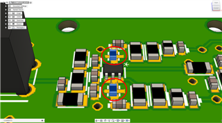
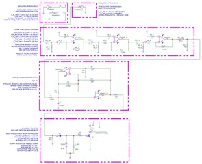
 RECEIVER DESIGN


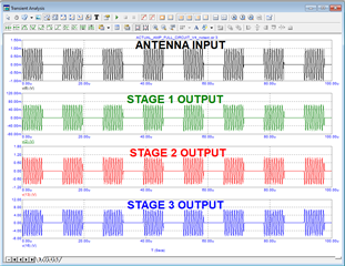
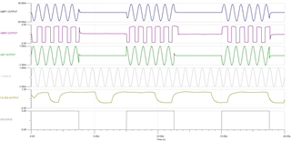
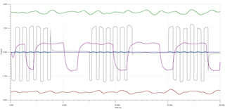
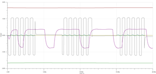
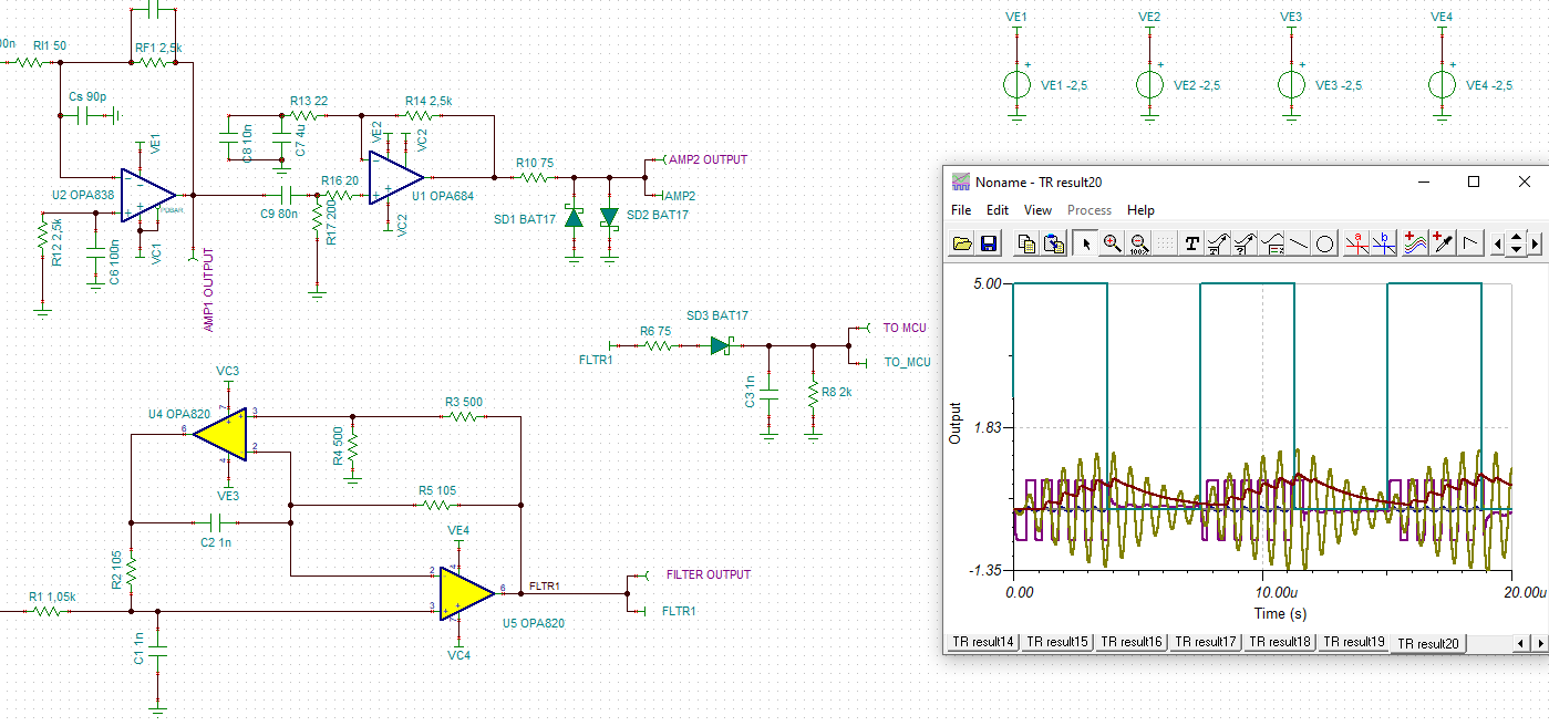
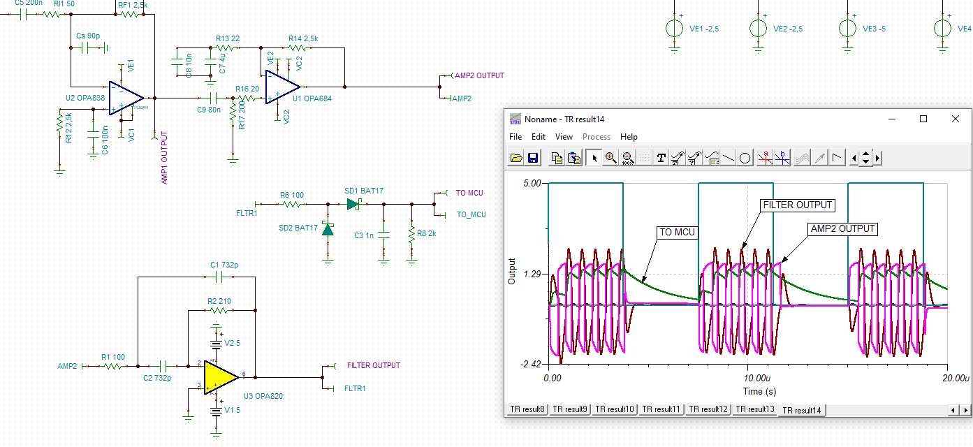
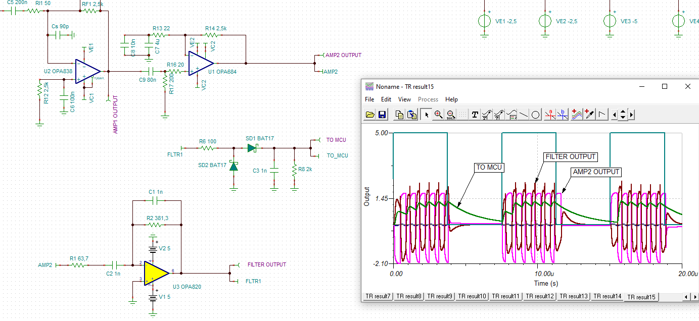
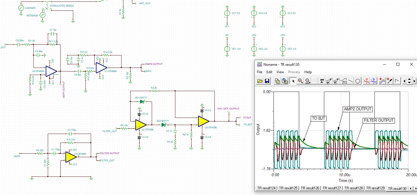
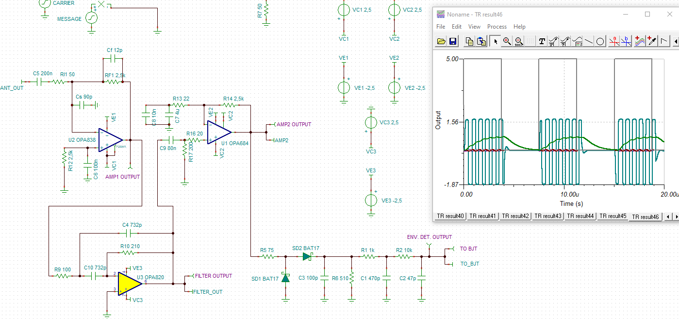
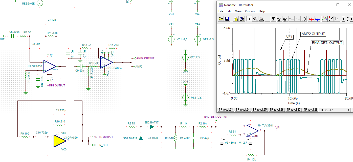
Question 1 – Why does the filter output look distorted?

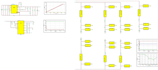
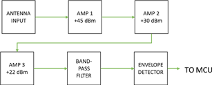
This topology is configured according to Figure 60 of the datasheet for the OPA820.  The filter has been designed for a cutoff frequency of 1.5 MHz with a Q of 10 according to the design procedure described in section 10.2.1.2.1 of the OPA820’s datasheet. 

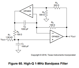
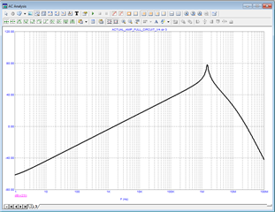
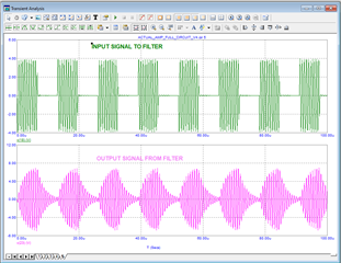
The AC response of the filter performs as expected.  However, the transient response is not acceptable for the following demodulation stage.  In ideal simulations, the high Q band-pass filter output “rings” when the carrier signal is removed, and “charges” when the carrier signal is applied.  What do I need to do to make the output look just like the input? 


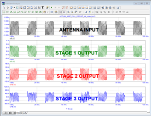
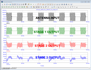
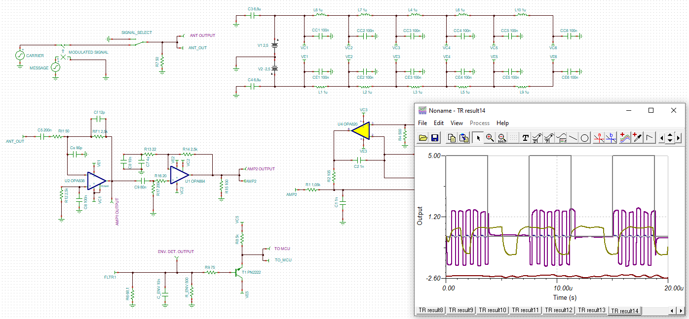
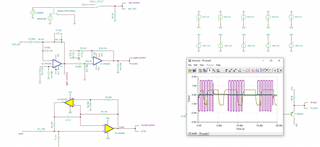
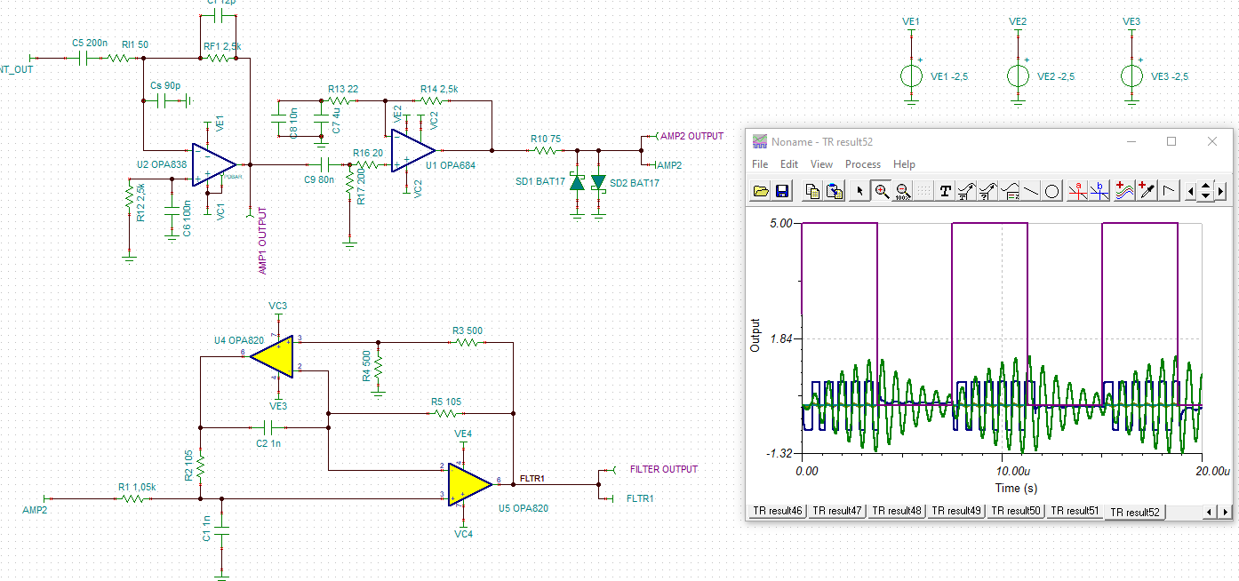
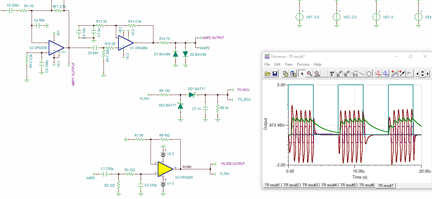
 Question 2 – Why don’t these opamps amplify as expected using Boyle Model?

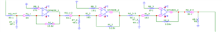
This topology is configured according to Figure 75 of the datasheet for the OPA838.  The amplifier has been designed for 50Ω Impedance, and is configured in 3 stages.  To reduce noise amplification, he first stage produces 50% of the total gain (45 dBm), the second produces 30% of the total gain (30 dBm), and the third produces 20% of the total gain (23 dBm).  The datasheet contains recommended resistor values for gains ranging from 15 dBm to 26 dBm.  As stage 1 and 2 require more than 26 dBm gain, resistor values have been derived.  Care has been taken to maintain the relationship between Ri and Rf displayed in table 2 of the data sheet. 

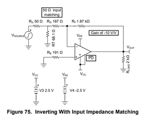
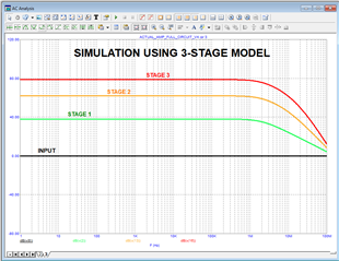
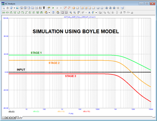
In more realistic simulations, using Boyle model for the opamps, the first amplifier stage amplifies the signal as expected.  However, in the 2nd and 3rd stage, the signal isn’t amplified at all, it is actually attenuated to the point that it is weaker than the input signal.  This does not occur with the more ideal models like the 3-stage model.  What do I need to do to fix this issue?  Is this some sort of impedance matching issue? 


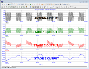
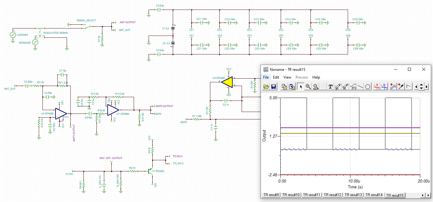
QUESTION 3 – Why don’t these amplifiers like larger signals?

Using the ideal model for the opamps, a small signal can be amplified as expected from 1uVpp to 10uVpp.  However, above 100uVpp, the amplifier does not behave as expected. It behaves as if it has been overloaded, or “jammed”.  How can I fix this problem? 


  • Morning Ryan, 

    You sure have a lot going on here, without getting too deep into it couple of observations

    1. Your high gain cascaded stages are broadband when you say you have a noisy environment - are you sure you don't want to do a little bit of bandlimiting in those stages to keep them from banging into the supply rails with out of band signals. 

    2. When you do that much gain in series, it is prudent to break the feedback loop through the power supplies using a pi filter on those supply decoupling from output to input, that shows up in this old app note I wrote, look at section 6 here - 

    www.ti.com/.../snoa367c.pdf

    3. You say Boyle model, the full Spice or TINA model is quite good, why don't you use that? 

    4. Your interstage coupling after the 1st one does not need to be doubly terminated 50ohm, don't take that insertion loss. 

    5. You appear to have a low power theme, and that OPA838 is certainly interesting for that in the 1st stage - if you want a lot of gain in an AC coupled path (no DC precision needs) look at the OPA683 and OPA684 - their higher noise does not matter after the 1st stage, 

  • Just to illustrate some ideas, see this OPA838 + OPA684 single 5V AC coupled design. I think the inupt referred noise is pretty high here and I do have some old circuits I did that can improve that, but that is much larger discussion - if this is good enough perhaps interesting, 

    3 V9 files and a word description, High gain cascaded stages 1MHz carrier.docx

    1374.Inverting high gain OPA838 with caps.TSC

    OPA684 non-inverting gain of 110 AC coupled.TSC

    Inverting high gain OPA838 followed by OPA684.TSC

  • Thank you for your helpful and quick response.  I think it solved 2 out my 3 problems.  Apologies my response wasn’t quite as fast.  I had to spend quite a bit of time going through all of the great observations and references you’ve provided.

    In summary, I am now using TINA, and have attached the model for the receiver.  TINA took some getting used to, but seems to be a great tool.  I have implemented the pi-filter network on the power rails, as well as the amplifier topology you describe in High gain cascaded stages 1MHz carrier.docx. 

    The attached TINA schematic for the receiver is much improved over the original.  The amplifier stages perform as expected in terms of gain.  They also seem to manage large (+24 dBm) and small (-56 dBm) signals well.  However, I’m still struggling with the following high-Q bandpass filter.  Referring back to my original questions:

    Original Questions:

    • Why does the third amplifier stage not amplify in “realistic” simulations using Boyle model?
    • Why do the amplifiers not manage large signals very well?
    • Why the distorted output from the high Q band-pass filter?
      • The high Q band-pass filter AC analysis looks great, but the transient does not look so good.


    RECEIVER.TSC

    1. Your high gain cascaded stages are broadband when you say you have a noisy environment - are you sure you don't want to do a little bit of bandlimiting in those stages to keep them from banging into the supply rails with out of band signals. 
    • If we can make this work, I think it is a great idea. I guess I didn’t want to do too much all at once since I couldn’t seem to get the amplification to function properly. 
    • Topology from High gain cascaded stages 1MHz carrier.docx was implemented as replacement for the amplifier stages previously described. I still have some questions about this topology, but I will ask those in a separate thread

    2. When you do that much gain in series, it is prudent to break the feedback loop through the power supplies using a pi filter on those supply decoupling from output to input, that shows up in this old app note I wrote, look at section 6 here - 

    www.ti.com/.../snoa367c.pdf

    • I have read this document and it was very helpful. Thanks for sharing!
    • I have implemented this in the attached TINA schematic.
    • I am having trouble determining the inductance of the baluns
    3. You say Boyle model, the full Spice or TINA model is quite good, why don't you use that? 
    • Thanks for keying me into the TINA software. I have downloaded it and I am using it now.
    • My main goal with this simulation/model is to eliminate any costly PCB redesigns later on down the road. I know the physical PCB plays a role in this as well, but I want to ensure that the schematic driving that layout is as optimized as possible. 
    4. Your interstage coupling after the 1st one does not need to be doubly terminated 50ohm, don't take that insertion loss. 
    • Thanks, I was having trouble rationalizing the need to reamplify something I had just amplified.
    5. You appear to have a low power theme, and that OPA838 is certainly interesting for that in the 1st stage - if you want a lot of gain in an AC coupled path (no DC precision needs) look at the OPA683 and OPA684 - their higher noise does not matter after the 1st stage, 
    • There is a low power theme, we are running on a finite battery power supply. That department hasn’t been completely optimized yet, but it’s good to have the headroom with the disable functions.
    • I have implemented the OPA684 as per High gain cascaded stages 1MHz carrier.docx
  • Just to illustrate some ideas, see this OPA838 + OPA684 single 5V AC coupled design. I think the inupt referred noise is pretty high here and I do have some old circuits I did that can improve that, but that is much larger discussion - if this is good enough perhaps interesting, 

    3 V9 files and a word description, High gain cascaded stages 1MHz carrier.docx

    1374.Inverting high gain OPA838 with caps.TSC

    OPA684 non-inverting gain of 110 AC coupled.TSC

    Inverting high gain OPA838 followed by OPA684.TSC

    Thanks for this walkthrough of the design procedure. This is almost exactly what I need, and solves 2/3 of the problems I originally had.  For my own learning/understanding, I would like to understand a little better how this topology works.  I really don’t understand the reasoning behind some of the components.  I’ve looked over the datasheets for the OPA838 and OPA683/4 and couldn’t find too much there.  I understand the gain/bandpass filter calculations in the first stage, but there are also some other components present which I don’t understand their purpose.  On the second stage, I’m even more confused.    Do you know of any datasheets where these topologies might have already been pretty well described?

  • Hi Ryan,

    your supply voltage filtering is heavily ringing. Look what happens when I set the ferrite bead inductances to zero:

    ryan_opa838.TSC

    If you actually want to simulate the supply voltage decoupling, then avoid resonances by introducing ohmic losses in the ferrite beads and ESRs in the decoupling caps.

    Kai

  • Of course you do want to use the full ferrite model which becomes more lossy going up in FMurata BLM21AG102SN1 with X2Y for power supply filtering forward filtering 2 stage.TSC- here is an example I did also using very high self resonance X2Y caps and full models. I did introduce 2.2ohm extrinsic between the electrolytic and X2Y at each DUT supply pin, pretty good job of attenuation - this file shows full part numbers in this example - signal path is righ to left here. 

  • This is pretty open ended question? 

    1. The CFA stage will lose BW quickly if I let the Rf get too high. 

    2. To hold it down, that meant the gain R needed to be pretty low

    3. To keep from loading the OPA838 output (bandlimiting also), I ran non-inverting in the 2nd stage

    4. but, loaded the OPA838 with a 200ohm termination which it likes and introduced a blocking cap

    5. That blocking cap goes self resonant, the series R into the V+ node deQ's that helping input stage stability

    Those sharp bandpass filters are going to have some start up issues I think. Normally we use those with sinusoidal carriers, square wave might look a little weird, You might try reducing the Q some - I have a design flow somewhere for that topology, see if I can find it

    You may have said already, but what is the BP target? Fo =10MHz I suppose, but Q

  • Hi Ryan,

    I prefer using individual Pi-filters at each OPAmp instead of arranging the ferrite beads and decoupling caps in a chain.

    I usually take 2µ2/X7R caps in 0603 (preferred) or 0805 package for the caps at the input and output of Pi-filter with the cap at the output of Pi-filter being connected closest to the supply voltage pins of OPAmp. Every millimeter counts!

    I avoid parallaling different cap values because of the risk of creating resonances. The ESR of the modern X7R caps is so low that heavy resonances can occur when paralleling unequal caps. If I really need to put two caps in parallel, I take two identical ones. But such a paralleling is very seldom.

    In former days for the paralleling tantals and ceramics were used and the high ESR of tantal sufficiently damped all the resonances. Tantals had to be used because they were the only source of high capacitances. And to overcome their lousy high frequency performance they had to be paralled by tiny ceramics. But with the todays high capacitance ceramics tantals are no longer necessary. As consequence measures have to be taken to deal with the very low ESR of ceramics, namely by avoiding the paralleling of unequal cap values.

    For the ferrite bead I take the "FBMH1608HM601". This is a "high current" ferrite bead. High current ferrite beads go into magnetic saturation at somewhat higher currents compared to standard ferrite beads, this is what they promise Relaxed. From the impedance versus frequency curve an inductance of about 1µH can be read out. Make no mistake, a ferrite bead is no coil. Because of the typical ohmic losses of a ferrite bead you should not talk about a pure inductance of 1µH. Anyway, ferrte beads show enough inductance and too little ohmic losses to still be able to cause heavy ringing when they series resonate with the decoupling cap.

    So very often I put a resistor in series to the ferrite bead. This also improves the filtering performance at the lower frequencies where the ferrite bead still doesn't work. The series resistor should roughly satisfy (remember, this is a ferrite bead, no coil) the condition

    R > SQRT (2L/C)

    which gives a minimum series resistance of 4R4, if a 100n decoupling cap is used. Or 1R, if 2µ2 is used. From this point of view a higher decoupling capacitance is better, provided it can still sit in a very tiny 0603 package. A 10µ cap in a 1206 package would not do the trick! Low package inductance is what counts more here.

    A higher decoupling capacitance is also wise when driving a heavy load. So a 2µ2/X7R/0603 decoupling cap is a good compromise in the very most cases. Y-caps might still give better results in the most demanding applications. But even little seeming layout mistakes can fully destroy their advantage.

    Pi-filters should always be mounted in a way that guarantees that all the components are sitting closest to each other. It's no good idea to put the ferrite bead distanced from the OPAmp and decoupling cap. The cap at the input of Pi-filter is not that critical and can be moved away from the ferrite bead a bit. But no too much. No more than a centimeter or so.

    If you do it right, the Pi-filter will fully decouple the load current demands from the OPAmp. The supply voltage line at the input of Pi-filter will look totally quiet and can be routed all over the printed circuit board without any problems.

    Kai

  • Well Kai, 

    Keep in mind this app is <3mA quiescent, not sure we need higher power ferrites

    Star vs cascaded filters? When I was doing that origina work with the CLC401 with a lot of cascaded gain, it seemed to make more sense to add up the supply attenation back towards the input stage - but either would probably work here. 

  • This is no high power ferrite but a high current ferrite optimally suited for supply voltage lines. And don't forget the load currents. R15 is 100R.

    The CLC401 showed a quiescent current of 15mA? So in the above application 5 x 15mA = 75mA would flow through the first ferrite bead in the cascade...

    Kai

  • Ferrite beads didn't even exist when I was doing that work. Or at least I was not aware of them in 1987

  • Thanks for the continued support on this.  Interesting discussion, and thanks for the options.  I'm doing my best to keep up with it.  I have modeled the pi filter network, and it does seem to clean up the power rails nicely.  please find attached TINA schematic.  I have yet to model the ferrite beads, but I plan to do so using the models in Murata BLM21AG102SN1 with X2Y for power supply filtering forward filtering 2 stage.TSC-.  Is this pi network good enough, or should i put some more immediacy behind the modeling of the ferrite beads?

    Previous

    Current


    RECEIVER-1.TSC

  • That murata ferite bead model I did was from their web site, I think it is pretty good. 

  • Hi Ryan,

    I would first try to make the circuit work with perfect supply voltages. I would add the supply voltage filtering later, in a second step. Divide and conquer Relaxed

    Kai

  • Copy that, I suspect my filter topology won't work even if the supplies are perfect.  We can come back to the supply discussion when we're ready.  

    I have attached an updated schematic with perfect voltages.  Still having trouble in the filter stages.

    RECEIVER-2.TSC

  • That murata ferite bead model I did was from their web site, I think it is pretty good.

    I'm having a little trouble getting my version of TINA to make a macro.  Probably just growing pains on my part.  This is what's slowing me down.  not sure if it is because i have a free version of TINA or something else.

  • You may have said already, but what is the BP target? Fo =10MHz I suppose, but Q

    I followed the detailed design procedure in the OPA820 for the high Q filter (section 10.2.1.2.1)

    Input parameters were Fo= 1.5MHz and Q = 10.

    We can reduce Q if necessary, but I would like to keep it as high as possible due to the noisy environment.  

  • Hi Ryan,

    removing the envelope detector and adding a Schottky diode limiter results in this:

    ryan_opa838_1.TSC

    Kai

  • Adding a simple passive envelope detector gives this (wine red curve):

    ryan_opa838_2.TSC

    Seems that the Q of bandpass is a bit too high, resulting in a too long settling time?

    Kai

  • Or like this, with a passive bandpass:

    ryan_opa838_4.TSC

    Kai

  • Thanks for the continued support.  I guess I'm just going to have to get used to the fact that I'm not going to be able to implement a filter with such a beautiful AC response as the one under discussion.  Thanks for the example above.  it looks like it works pretty well in transient simulations.

    In an effort to find the best Q bandpass that i can bolt on to the output of the amp stage, I've put together a couple of topologies.  The infinite gain multi feedback band pass (filter 3) seems to preform pretty well.

      FILTERS.TSC

  • Hi Ryan,

    here in combination with the pre-amplifier and the envelope detector:

    In any case, reducing the Q of bandpass filter is of benefit here. Lower Q = faster settling.

    Kai

  • Thanks Kai, i noticed you are using +/-5v for the filter.  The amps are running at +/-2.5v, was that intentional?  Just curious because i cannot seem to get the 2stage amp + filter combination to work without using +/-5v for the filter, as you've done.

  • Yes, was intentional, because of the voltage drop across SD1.

    Kai

  • Ok, got it, thanks!  is that something we will work out later when optimizing, or am i going to have to source some 10V power in addition to the 5V?

    The envelope detector needs to drive something that will invert it's output to make a dominant bit low and clean up the rise/fall time.  We need <1.5 us for the rise and fall.  I have been using an NPN BJT for this in the past. 

    is there anything we can do to clean up the edges and make it look as "square" as possible?  maybe a comparator?

     RECEIVER-3.TSC

  • Hi Ryan,

    here with an active envelope detector and exclusive +/-2.5V supplies:

    ryan_opa838_5.TSC

    Kai

  • Hi Ryan,

    I would mount the bandpass filter in front of the gain stage with the output clipping, because it's impossible to filter out noise and interference when the clipping once has taken place. It also simplifies the envelope detector design, because the settling time of bandpass filter plays no longer an all too significant role.

    To get a symmetrical envelope detector signal I have drastically reduced the rectifier time constant and added a passive two pole low pass filter:

    ryan_opa838_6.TSC

    The envelope detector signal is big enough to be able to be handled with a simple comparator. An active envelope detector isn't necessary.

    I would add a comparator with a threshold voltage of about 430mV. This should give a symmetrical output signal:

    Kai

  • Like this, for instance:

    ryan_opa838_7.TSC

    The comparator is only powered by a single supply voltage of 2.7V in the simu, because the model obviously doesn't like a bipolar supply voltage. But in reality the TLV3501 should be able to be powered by +/-2.5V.

    Of course, this here is no ready solution. A lot might have to be optimized. For instance, the hysteresis of comparator and the ripple of envelope detector should fit together. And, probably, there's no need for such a fast comparator like the TLV3501.

    Kai

  • Thanks for the help Kai.  Apologies for the slow response, I was out of the office for a couple days.  I have reviewed and tweaked a few resistor values in the envelope detector, as well as the reference voltage on the comparator.  It looks pretty good, and meets the design requirements.    

    I think we can say we have a viable "ideal" design.    

    Also, I just realized i made a mistake in calculating the message frequency, I had calculated message frequency based on the period of a half cycle (smh).  The message frequency has been updated to 67KHz (from 133 KHz).  This give the envelope detector a little more time to charge.

    2870.RECEIVER.TSC

  • I am working on updating the power supplies to something more realistic.  

    In reality, there is a of jewelry between the prime power supply and these op amps.  Do you think I need to model the entire power supply chain to produce accurate results?  

    Below is an illustration of the power supply that this receiver is ultimately connected to.  

  • Hi Ryan,

    yes, 67kHz makes more sense to me than 133kHz Relaxed

    Provided you adopt the recommended wirings of regulators given in the datasheets, I wouldn't simulate the whole power supply chain. Referring the LM2596 I would add the "optional post ripple filter" shown in figure 9-10 of datasheet, though. And follow the layout recommendations.

    I have made very good experience with the LM2674, by the way, which I use as a pre-regulator like you. Do you actually need a 3A switcher?

    Referring the supply voltage filtering of OPAmps, I have already given some recommendations. Important is to mount a 0603 or 0805 packaged 2µ2...4µ7/X7R cap close to each supply voltage pin. Then take my or Michael's ferrite bead to form a low pass filter. Both are well suited. If you follow the path of using an individual Pi-filter at each OPAmp, I would add a small resistance in series to each ferrite bead to dampen ringing. But that's my personal taste.

    Simulating this whole supply voltage decoupling stuff together with the signal processing may become difficult, because the simulation seems already to run on full blast only with the signal processing. So I wouldn't do this. But you can easily simulate the pure decoupling performance as Michael showed 4 days ago. Look for resonance spikes in the frequency response which you should avoid. If your curve is as flat as Michael's curve, then you have done it right.

    The only issue I see, if at all, is the very high gain of U1 and U2. If any problems arise in the protoype, you might want to split the high gain of U1 (or U2) onto two amplifier stages each, with equal gain. But this is only something I would keep in mind for the testings.

    Kai

  • Thanks Kai, working on the power supply as we speak.  I will stick to modeling the supplies separate from the signal processing.

    Regarding the power supplies, I don't need 3A for the 5V supply, that's for sure.  The 5V rail is also supporting the MCU and sensor packs, for a combined total of 150mA.  The 24V rail draws 0.5A max.  I was a bit strapped for time, and already have some experience with the LM2596.  Since i was configuring two voltage supplies, i cut a corner and stuck with the same LM2596 for both supplies. I hope that doesn't cause any issues and is just an inefficiency.  

    in case you're interested, i have attached the EAGLE schematic with actual part numbers for the power supply (sorry, no TNA simulation on it yet).

    POWER.pdf

  • Here are the two options for power supply filtering.  For the purposes of the 1.5 MHz signal, they're both acheive significant attenuation.  

    PI-POWER.TSCFE-POWER.TSC

  • Any suggestions on how to create VB4?  I've had a look, and couldn't find any reference voltage ICs that would go down to 0.4v.  I went ahead and tried a voltage divider network, and was surprisingly able to get a solution from the solver, although it took a few hours.  it doesn't look like the voltage divider network is stable enough to create a good reference voltage. 

    RECEIVER-REAL-power.TSC

    .  

  • Hi Ryan,

    I would not do it with a pseudo ground genereator. Keep in mind that the source impedance at high frequncies of such chips rises to dozens of Ohms or even more. So the output of TLE2426 might not be able to source and sink the high frequency contents of "ground currents" flowing into the pseudo ground. In HF applications like this I would prefer a true ground which is not limited in sourcing and sinking currents. 

    I would power the HF OPAmps by the help of an unregulated +5V to +/-5V DC/DC converter and use voltage regulators to generate the +/-2.5V supply voltages.

    Also, the series resistances are meant to be installed in series to the ferrite beads, as if a ferrite bead showing a much higher equivalent series resistance would be chosen.

    Kai

  • Thanks Kai  Apologies for dragging this conversation on, i am tired of being surprised when I put a PCB together :)  I'd like to get it right.  This thread is going to quickly turn into a power supply discussion based on my next question.  :)

    I have a few different designs I'm working on, and I've also just discovered the "WEBENCH".  It looks like there are quite a few ways to get the +/- 2.5 V supply to the amps.  Also, please keep in mind, before I started this post, i had just completed a redesign of the power supply system (PCB and all).  So I am a little hesitant to redesign it again.  But, if that is what needs to happen, I'll make it happen.     

    Regarding your last comment, I am tying to understand the flow from battery to opamp.  it sounds like i need to create a +/-5V using a buck converter, as is described in SLVA369A www.ti.com/.../slva369a.pdf

    Below is an illustration of my understanding.  Can you let me know if this is an accurate representation of what you describe?

    Also, using the existing 30v-8v-5v power supply, would something like this work?


  • Dear Ryan, there's absolutely no need to apologize Relaxed

    With the +5V to +/-5V DC/DC converter I meant something like this:

    https://www.mouser.com/ProductDetail/RECOM-Power/RB-0505D?qs=YWgezujkI1KtSVTjr6rRjg%3D%3D

    And I would choose the first scheme.

    Kai

  • Thanks Kai.  The +/-5V converter is much easier your way!  I contacted RECOM and unfortunately they don't have a spice model available, they're working on it.  They did offer me some free samples though!  Also, I'll probably need to move to a different module due to the temp limit on their deceives topping out around 100 °C.  

    I have attached a schematic of the power supply design.  I am not sure what to do with the two +5Vout rails.  Can i use the TPS71725 for anything other than powering the r1dx-0505?  i.e., could i use it for OP4 and other devices that need +5v?

    3835.POWER SUPPLY.TSC

  • Hi Ryan,

    the LM27762 could also do the trick. You could generate +5V with the LM2596 and generate +/-2.5V by the help of LM27762. The +5V for the comparator could be taken from the +5V of LM2596.

    Kai

  • That simplified the system a lot.  I have used WEBENCH to select a better module (LM60440D) for switching from 30V to 5 volts.  Then, as you suggest, I use the 5V output and a LM27762 to generate the +/- 2.5V rails. 

    The comparator (OA4) is powered by the +5V from the LM60440D, and the 3 amplifiers (OA1-3) use the +/-2.5V rails from the LM27762.  I am using the pi-filter network on all of the op amps.  The ferrite bead option seemed to not yield significantly different results, and would be more complicated to implement.

    I have attached the tina schematic showing this circuit.  I am not able to get the transient analysis to complete with all of the devices in one circuit.  However, i am able to get them to function properly in isolation.    

    RECEIVER_POWER_SUPPLY.TSC

    LM27762.TSC

    LM60440D.TSC

    7853.PI-POWER.TSC

  • Hi Ryan,

    looks good so far Relaxed

    I am using the pi-filter network on all of the op amps.  The ferrite bead option seemed to not yield significantly different results, and would be more complicated to implement.

    I hope you will take ferrite beads at the places the simu shows the 10µH chokes? A classical 10µH choke would show a much higher parasitic parallel capacitance (winding capacitance !) which you haven't modelled yet and as result a much lower resonance frequency compared to the ferrite beads Michael and I have chosen. As consequence the filtering performance at the very highest frequencies would degrade. So please use ferrite beads Relaxed

    Kai

  • Thank Kai, I'm having a little bit of trouble following the pi-filter vs. ferrite bead discussion.  I was thinking that they were two options that achieve the same thing, in different ways.  I see now that was not correct.  Why was i modeling the pi-filter instead of the ferrite beads?  Was it just to simplify the representation of the ferrite bead?  I've studied the model Michael sent, and I've made an illustration of my understanding of it.  I'm pretty sure it's a wrong understanding :).  so, feel free to correct my thinking.  Also, I don't understand where the two 2.2uF caps and the resistor that limits "ringing" are supposed to fit into this model. Can you help me understand that too?  Thanks again!

    Murata BLM21AG102SN1 with X2Y for power supply filtering forward filtering 2 stage (4).TSC

  • Hi Ryan,

    L2=3nH is the parasitic series inductance of C2 including the layout inductance of ground plane. L2 of naked C2 would be less than 1nH.

    L3=50pH is the parasitic series inductance of C3. As being a Y-cap L3 is very much smaller than the inductance of a standard 0603 cap, like L2 .e.g. But layout mistakes can entirely ruin this advantage.

    The ferrite bead is formed by L1, R2, C1 and R1. L1 is the indutance which dominates at low frequencies. C1 models the parasitic parallel capacitance which is responsible for the position of resonance frequency. R2 models the maximum impedance at the resonance frequency. R1, finally, models the equivalent series resistance (ESR) of ferrite bead at DC.

    L4, C4 is just another L2, C2.

    A classical Pi-filter would look like L4, C4 on the left and L2,C2 on the right with the ferrite bead in between. And the additional series resistance recommended by me would be in series to the ferrite bead, effectively increasing the value of R1, or by other words, this series circuit would be framed by L4, C4 and L2,C2.

    Michael has added the RC filter "R3 and L3, C3" to the Pi-filter "L4, C4 and R1, L1, R2, C1 and L2,C2".

    Kai

  • Thanks for the explanation Kai, that really helped a lot, it all makes sense now.  I have attached the TINA schematic of one of the +2.5V supplies for the opamps.  I have used macros to model the various components you and Michael mention above.  From what I can tell, the models should be identical, but I'm only getting close, not identical results.  I'm not sure why this is happening.  

    I have also added the series resistance "R_Kai" between the ferrite bead and the output cap (C2).  I have set it to 0 for the purposes of creating an apples to apples comparison with Michael's model.  

    RAIL.TSC

    Thanks

    Ryan

  • Here is a look at the entire power supply, from battery to op-amp power rails.  

    POWER_BOARD_RX.TSC

  • Looks good. Unfortunately I cannot open your TSC file, maybe because I have an elder version of TINA-TI.

    Kai

  • Hi Kai,

    I'm using the following version of TINA:  Version 9.3.200.277 SF-TI

    I have saved the schematic as a Tina-V7 schematic, maybe that will work?

    POWER_BOARD_RX_TINAV7.TSC

  • Hi Kai,

    I've had a go at arranging the components on a PCB.  To simplify, I have attached a picture of the power supply only for one op amp.  The other op amps can be configured in the same manner.  Since I'm using the X2Y caps, in addition to the FE bead/pi filter, I have placed them as close as possible to the power rails of the OA.  You mention above placing the 2.2uF caps as close as possible to the pins.  I'm assuming you weren't envisioning implementing x2y caps when you were saying this.  

    Also, I use EAGLE for the pcb side of things.  Does TI have a go to PCB design tool/simulator that would facilitate easier collaboration?

  • Hi Ryan,

    if you use an Y-cap, try to mount the Y-cap (but not the resistor or ferrite bead) as close as possible to the supply voltage pin of OPAmp. Only by this you get the best benefit of ultra low parasitic inductance of Y-cap.

    If you don't want to use Y-caps, you could do it like shown in this example layout I created for another thread:

    Look how close C2 and C4 are mounted to the OPAmp.

    Kai

  • Thanks Kai, I appreciate the explanation.  Since I've already modeled the X2Y caps in TINA, built the EAGLE Library / Schematic / PCB, and identified parts on Mouser, I think I'm going to stick with the X2Y Caps until I have a good reason not to.  What do you think?

    Based on your last reply, I have updated the position of the X2Y caps, which actually helped slim down overall footprint of the opamps/passives.  Please take a look and let me know if you have any concerns

    Thanks,

    Ryan