This thread has been locked.

If you have a related question, please click the "Ask a related question" button in the top right corner. The newly created question will be automatically linked to this question.

TLV9152: Input behaviour during shutdown

Part Number: TLV9152

The TLV9152S includes a shutdown function.

I'm willing to use this amplifier to adjust the input voltage received from a standard voltage reference of 2.5 V.
The adjusted output voltage of the TLV9152S (for example 5 V) will be buffered by a following 1:1 amplifier which also has a shutdown feature.

This second amplifier might be destroyed if any input voltage is applied during shutdown.
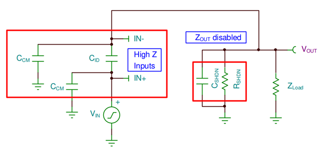
Therefore I’m planning to switch-off the TLV9512S into shutdown mode. I‘m expecting that the output of the TLV9152S will go into an high impedance mode, i.e. no longer delivering any current to the following OP – fine this second OP will be saved.

But now I have the same problem with the inputs of the TLV9152S. With this amplifier being in shutdown mode, the feedback loop will not be closed any longer. Therefore, the voltage difference between the 2 input pins will be undetermined.

Since the TLV9152S being still powered with its supply voltages, the input voltage will be in the specified voltage range. But what effect will be seen, caused by the undetermined voltage difference between the two input pins?
And what currents are flowing into the +In of the TLV9152S (as function of the applied signal voltage)? If these input currents are greater than the quiescent current of the TLV9152S the reduction of supply current due to shutdown will be reduced significantly.

Could you please advise me some possible solution?

  • Hi user1505382,

    Glad you are taking a look at using the TLV9152S in your design! 

    To clarify, you are using the first amplifier to set an input signal to a 2.5V reference voltage, then using the second one as a buffer? 

    Since the TLV9152S being still powered with its supply voltages, the input voltage will be in the specified voltage range. But what effect will be seen, caused by the undetermined voltage difference between the two input pins?

    You can actually determine what the voltage will be! To determine what the input pins voltages are we need to make a simplified model of the amplifier in shutdown. The model I have shown below is Figure 8 from the Shutdown Behavior in TLV90xxS Operational Amplifiers application report. While the application report focuses on the TLV90xxS family of devices it will still apply to the TLV9152S. 

    This model is specifically for a buffer configuration. Here we have an input signal being applied to noninverting pin, IN+, and a load, Zload, connected to the output. When the op-amp goes into shutdown, the voltage on the output will get discharged through either Zload or Rshutdown, pulling the voltage on the output and inverting input pin, IN-, to ground. 

    And what currents are flowing into the +In of the TLV9152S (as function of the applied signal voltage)?

    The current flow should be very low, at the voltage levels you describe. The input resistors in the image I shared above, aren't there but can be found in the datasheet in page 11. There you will see two different input impedance values. 100Mohms for differential resistance, and 6Tohms for the common mode resistance. You can calculate what the expected current will be as a result of the difference in voltage across the inputs. 

    Let me know if you need any further assistance! 

    Best Regards, 

    Robert Clifton 

  • Thank you for your really helpful answer.

    Just to get it right, my understanding:

    With 2.5 V at the +In (and the feedback-lopp disabled, i.e. 0,0 V at the -In) the current into the device (at +In) will be 2.5 V / 100 MOhm = 25 nA, which is really negligible. So there seems to be no protection diodes inside this OP which will switch on generating any higher current.

    This will be fine, so my plasnned design should work.

    Thank you again.

  • Hi user1505382,

    I'm glad to have helped you but also apologize for not talking about the protection diodes in my original response. There are indeed protection diodes in this device. However, in my simplified model, I didn't include them as I had calculated that the voltages seen at the input would not extend beyond the supply voltage of the device. 

    If you do end up having a worse case scenario where the voltage on the input that goes above the supply voltages, including a resistor in it's path would help reduce the current going through the protection diode(s)! I would recommend including one in the noninverting pin as a safety precaution to ensure a more robust design!

    Best Regards,

    Robert Clifton 

  • Hi Robert,

    it would also be interesting to know whether there are protection diodes (or a similar protection scheme) between the inputs of TLV9152 Relaxed

    Kai

  • Thanks again for your helpful answer.

    These protection diodes, mentioned by you, should be no constraints for my planned design.
    At least, if I have understood you right.

    Protection diodes versus the supply voltage will not switch on, if my signal input voltage is lower than the V+ and higher than V-.
    And this will be the case with the signal input voltage to be about 2.5 V, V+ to be between 6.0 V and 8.0 V and V- to be 0,0 V.
    I.e. my input voltage at +IN will always be well within the voltage range between V+ and V-. More than 2 V distance to either rail.

    What was my concern are any possible protection measures by using differential diodes between +IN and -IN, which are quite common in many operational amplifiers. With the –IN going down to 0.0 V the difference between the input signal at +IN (2.5 V)  and the voltage at –IN (0.0 V) will be about 2.5 V and this might switch on any protection diode between these two pins, if there will be any.

    However, if I understood you right, there are no protection diodes between +IN and –IN, but protection diodes between +IN and V+, and between +IN and V-, and also between –IN and V+ and between –IN and V-. Therefore, these protection diodes will not interact with my planned function, and my design should work well.

    Thank you again.

    Best regards,

    Hans-Ludwig Reischmann

  • Hi Hans-Ludwig and Kai,

    An easy way to determine whether there is back to back diodes, or differential diodes, on the inputs of an op-amp, would be to look at the absolute maximum rating of the differential input voltage. Back to back diodes would clamp the voltages at 0.3V to 0.7V.

    In the case of the TLV9152S, the maximum differential voltage is the supply voltage plus 0.2V. This tells me that for the TLV9152S, there is no back to back diodes on the input! 

    Best Regards,

    Robert Clifton 

  • Thank you again, for this helpful answer

    Hans-Ludwig