This thread has been locked.

If you have a related question, please click the "Ask a related question" button in the top right corner. The newly created question will be automatically linked to this question.

INA828: Differential output

Part Number: INA828
Other Parts Discussed in Thread: THP210, XTR116, ADS1258-EP, ADS1278-EP, ADS1298R, INA826EVM, OPA828, ADS1261, ADS131E08, TINA-TI, OPA191

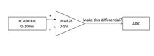
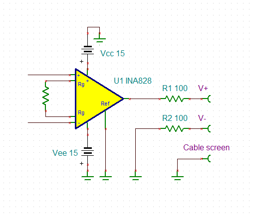
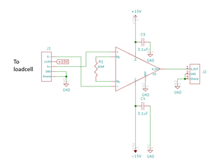
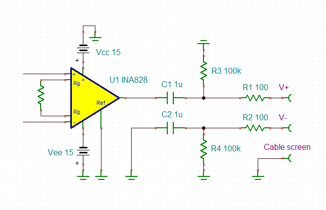
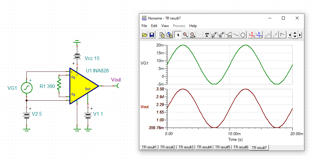
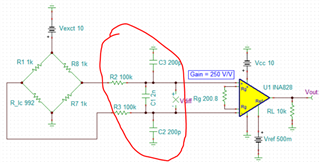
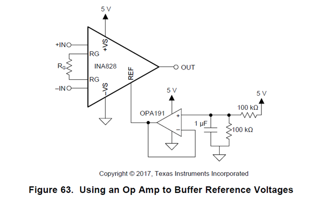
I have a loadcell which gives a differential output of 0-20mV with the INA828 connected to this to produce an amplified single-ended output of up to 5V which is connected to an ADC. I would like to know if there are any solutions for getting a differential output from the amplifier? 

  • Hi Esther,

    Thanks for your post, I can help. You cay consider taking a look at our fully-differential IA THP210: https://www.ti.com/product/THP210 

  • Hi, 

    Thanks for the suggestion. I was also wondering whether this step is redundant for my current setup. My concerns are about noise and EMI/EMC

    Currently, my signal input comes from the loadcell which operates on a strain gauge full bridge. My understanding is that the amplifier should have high impedance inputs to ensure that the loadcell signal(0-20mV) is not compromised, thus the use of the INA828 to amplify the signal.

    However, since my signal will be travelling some distance(not more than 2m, probably between 50cm-1m), I was wondering whether a single-ended signal would maintain its signal integrity or if it would be adversely affected by noise. Thus, I was looking for a differential amplifier to convert the single-ended signal to a differential signal before it travels some distance away to the adc (delta-sigma). 

    This feels rather redundant to me though since I am converting a differential signal to a single-ended signal and back to a differential signal again. Thus, I thought of a few alternative ways and would like some advice on whether these are feasible.

    1. Directly send the differential loadcell signal(0-20mV) to the delta-sigma ADC. 
      1. Would the signal be affected by noise since it is such a low level signal to the extent that it would be unreadable?
    2. Directly send the single-ended output from the INA828 to the delta-sigma ADC without converting it to a differential signal again (forgoing the THP210).
      1. Would the signal be affected by noise or couple to other components to produce noise which would affect the performance of the setup, especially since I would have 16 of such signal chains running in parallel?
  • Hi Esther,

    directly sending the signal of load cell over a distance of 2m would be the worst of all scenarios. I would take an instrumentation amplifier close to each load cell. After the amplification there would be no need for differential signalling anymore. But even if you insist in differential signalling, so called pseudo differential signalling would also do, if the cable length is only 2m:

    Can you tell more about your application? How are the 16 channels routed? Are they powered by the same supply? Are they seeing the same signal ground also at the load cell side? A wiring scheme would be good. I ask because of avoiding hum loops.

    Kai

  • Hi Esther,

    Kai provides some really good suggestions. Please help provide extra detail about your set-up. A schematic would be very helpful. 

  • Hi Kai,

    thanks for the suggestions.

    My circuit for each amplifier is something like this. 

    I will have 16 of such setups and the outputs would travel through individual cables to the adc. All the boards will get the same +15V and ground from the power supply(ie in parallel). The -15V for the amplifier's negative power input and 10V for the loadcell is converted on the board itself. Each loadcell will get its ground from the amplifier board which takes its ground reference as the ground input of the power supply to the board. My design isn't fixed yet so I'm open to any suggestions for improvements!

  • Hi Esther,

    I am with Kai and Tamara's suggestions below that the application may require to amplify the input signals that are closed to the transducers (load cells). The application will require up to 250V/V in order to gain up input signals from transducers. 

    I would take an instrumentation amplifier close to each load cell. After the amplification there would be no need for differential signalling anymore. But even if you insist in differential signalling, so called pseudo differential signalling would also do, if the cable length is only 2m:

    The data transmission of the remaining 2 meters may depend on the application's operating environment. If these signals have to transmit over a noise environment, such as motor driving environment, ovens, switching power supplies, inductive and capacitive loads etc., then a differential signal pairs or 4-20mA current loop ( XTR111, XTR116/ XTR117 etc.) will be better choices. If the analog signals are transmitted via low-noisy environment, single-ended or pseudo differential signals may work. Please let us know the application's operating environment. With differential signal pairs, everything is doubled as in wire bundle sizes, required ADC channels + other peripheral drivers. Maybe there are other options to transmit the data from the loadcell to the MCU. 

    If you'd like to use differential op amp configurations, you may consider the following options, including THP210 fully differential amplifier suggested by Tamara. 

    https://www.ti.com.cn/lit/an/sbaa264a/sbaa264a.pdf?ts=1644370960308&ref_url=https%253A%252F%252Fwww.google.com%252F

    https://www.ti.com/lit/an/sbaa265/sbaa265.pdf?ts=1644299477323&ref_url=https%253A%252F%252Fwww.google.com%252F

    https://www.ti.com/lit/ug/tidu038/tidu038.pdf?ts=1644361971044&ref_url=https%253A%252F%252Fwww.google.com%252F

    Please tell us more about the operating environment. BTW, is your loadcell is configured via Wheatstone bridge for the application?

    Best,

    Raymond

  • Hi Raymond,

    Thanks for the input. For my operating environment, the amplifier +loadcell setup would be close to the motors but further from the motor drivers. I probably won't be sending the signal over the whole 2m, more likely around 50cm ish so the amplifier +loadcell setup would be closer to the adc than the motor drivers which are around 1m away. However, the signals would possibly be run next to the cables(which are shielded) between the motor and motor driver. My loadcell is configured via Wheatstone bridge. 

  • Hi Esther,

    running the signal cables from the load cell amplifiers close to the motor driver cables is not at all recommended, even not with the best set-up and the best common mode rejection measures, just because the symmetry of any cable for differential signalling gets lost when coming with the interferer too close to this cable. So, in any case, you should avoid this. Also, you will need proper shielding of the load cell and load cell amplifier. The shielding enclosure and the cable screen should form an continuous and uninterrupted Faraday shield.

    What the best way to proceed is, also depends on the ADC. What are the inputs of this ADC? Single ended, true bipolar (for +/- differential signalling) or pseudo bipolar (for +/+ differential signalling)?

    There's another issue: You mentioned that the -15V is generated from the +15V supply? I guess by a DC/DC converter or charge pump inverter? If this is the case, switching noise can degrade the performance of load cell amplification. In any case proper filtering will be needed to get a clean, stable and noise-free negative supply voltage.

    Can eventually the negative supply voltage be omitted? Can you go with single supply? Can you show a schematic also showing the ADC section?

    Pseudo differential signalling is almost as effective as true differential signalling, but way simplier. The crucial point is, that both source impedances have to be exactly matched in the frequency range of interest. This is why R2 was added by me and why R2 should equal R1. "V+" and "V-" are to be connected to a shielded twisted pair cable then.

    But again, what the best and simpliest way to proceed is, also depends on your ADC.

    Kai

  • Hi Esther,

    As Kai suggested, you may go with the load cell's front end as shown in the simulation below. If the +15V is regulated out of a linear LDO, you may use as is. If it is regulated from a switching power supply, then you may consider to filter it out further and reduce to 10-12Vdc to reduce noise and ripple. In other words, it will be beneficial to simplify and lower the noise at the instrumentation and load cell input stages, also make it as small as possible so that the sensing system may be able to be shielded effectively (I did not configure the gain stage properly, if you are looking for 0-5V range for your ADC. This is just an example.). 

    INA828 0-20mV 0-5V Load Cell 02092022.TSC

    If the load cells are surrounded with larger or industrial motors, you may consider to use ferrite beads/core to eliminate additional EMI/EMC noises. 

    Regarding to the output coupling, I will go with Kai's recommendation. If the signal cable bundles are shielded, you may go with single-ended inputs to ADC. 

    Best,

    Raymond 

  • Hi Kai and Raymond, 

    Thanks both for your suggestions.

    When you mention proper shielding for the loadcell and amplifier, does that mean they should be enclosed such that they are separated from my other components which are all in the same enclosure already? I am currently looking for an ADC as well since the previous one I was using did not have enough channels, thus I don't have a schematic to show you at the moment. I am currently looking at either ADS131M08S, ADS1258-EP, ADS1298R or ADS1278-EP as I would like to get at least 1k samples per channel and I would be reading 8 signals per ADC.

    In terms of the input to the ADC, I have not decided on one yet since my signal could possibly fall in the slight negative range ~ -0.1V, due to the zero balance of the loadcell. In the same vein, I would still require a negative supply voltage since my loadcell could produce a slight negative voltage.

    When you mention proper filtering for the negative supply voltage, would capacitors be enough or are there other components I should be considering as well? Also, I'm not to sure what you mean by frequency range of interest, would it refer to the sampling frequency of the ADC or the frequency band of the amplifier or the signal frequency or something else? 

    For this simulation, may I ask if the values chosen for the input to the amplifier are calculated in some manner or just general values I could possibly use?

  • Hi Esther, 

    For this simulation, may I ask if the values chosen for the input to the amplifier are calculated in some manner or just general values I could possibly use?

    On p.7 of the INA826EVM, you will find sections how to configure the differential and common LPFs, see the link below. 

    https://www.ti.com/lit/ug/sbou115c/sbou115c.pdf?ts=1644468695227&ref_url=https%253A%252F%252Fwww.ti.com%252Ftool%252FINA826EVM

    When you mention proper shielding for the loadcell and amplifier, does that mean they should be enclosed such that they are separated from my other components which are all in the same enclosure already?

    When you are able to shield your load cell and OPA828  and the amplification circuit in Faraday cages (360 degree complete shielding around a cable bundle), it will protect against from static electrical charges and the electromagetic changes from flux changes of a motor. With the shielding protection, EMI/EMC coupling onto the sensing circuitry will be reduced to a minimum. You do require to balance the input resistance and capacitance of load-cell, resistance and cable length etc., and it may be a good ideas to use X2Y capacitor in your LPF filtering scheme in front of OPA828.   

    https://www.mouser.com/catalog/specsheets/johanson_johas00924-1.pdf

    You mentioned about the Wheatstone balancing: You may consider the following approach to null out the sensing circuit. And  you do not need negative supply voltage to do that. 

    Balance Wheatstone Bridge 02102022.TSC

    If your ADC and/or remaining circuitry is far away from the motor generator, the circuit may be ok to operate operate without shielding.  You can monitor the ADC's LSBs once you have optimized the input coupling to ADC and sampling circuits.  

    Please let us know what ADC you will be selecting and using. There are considerable know-hows about reducing the coupling noises between analog signal chains to ADC (you do not require high speed sampling, but you need up to 16 channels or more for the application).

    Kai will know a lot more than I do. Or you may send an E2E inquiry to our ADC supporting team. Please do tell what your requirements are in ADC. There are many approaches to handle this task. 

    If you have other questions, please let me know. 

    Best,

    Raymond 

  • Hi Raymond,

    Thanks for the reply. In terms of ADC, I am planning on using 2, each sampling 8 pseudo differential inputs as Kai has suggested at minimally 1k samples per input per second. I am looking at 24 bit ADCs with as high an ENOB and resolution based on the sampling speed I will operate the ADC at to get 1k samples per input ie at least 8ks/s. I think I will pop by the E2E for ADCs too and get back to you guys on the ADC I have chosen. 

  • Hi Esther, 

    Since you are dealing with 24bit ADC, you will need suggestions from ADC team to have a lower noise floor in the DAQ end. The 1LSB in 24 bit ADC is at 5V/2^24 = 298 nV range, and this is an ultra precision sensing application. In addition, you need need to pay attention to the PCB layout and minimize EMI/EMC couplings from external noise sources.

    Best,

    Raymond


  • Hi Esther,

    Also, I'm not to sure what you mean by frequency range of interest, would it refer to the sampling frequency of the ADC or the frequency band of the amplifier or the signal frequency or something else?

    It refers to the frequency range of signal to be transmitted. If your signal frequency range is DC to 100Hz, e.g., then the OPAmp would provide an almost zero output impedance and the R1 = R2 = 100R would give a perfect match. But if you would provide AC coupling by the help of a high pass filter, example given, you would need to "mirror" the high pass filter as well, to give a perfect match:

    Again, this is only an example. It does not at all mean that I do recommend AC coupling here.

    Another issue was, when your signal frequency range is so high that the OPAmp is no longer providing a zero output impedance at the highest frequencies. Then, it can be better to do true differential signalling by the help of another OPAmp (dual OPAmp preferred). But this doesn't seem to be the case here. I merely mention this to answer your question.

    Esther, from my understanding the critical point here is the load cell section and it's not so much of interest how you drive the ADC. Or by other words, if the signal integrity has already been ruined in the load cell amplifier, then even an ADC with true differential inputs does not have any chance to cure the mistake any more. So I would focus on the load cell amplification.

    Unfortunately, I dont know your application in detail. But if things are not too complicated, I would take an instrumentation amplifier, run it with a single supply and apply an offset voltage to the REF pin. The offset voltage could be about 1/4 of the reference voltage of ADC to allow some negative going load cell signal. Then, I would transmit the signal by the help of pseudo differential signalling. At the receiver side a simple "one-OPAmp" diffential amplifier could do the common mode rejecting of cable noise and driving the single ended input of ADC.

    As I already mentioned, the most critical point will be the load cell amplification. Keep in mind, that if you glue the load cell directly on the motor chassis or parts which are galvanically connected to the motor chassis, the potential of motor chassis should not differ all too much from the signal ground of your load cell amplifier. If this is not the case and between these both potentials noise is present, an unsane portion of this noise can be directly coupled into the signal chain of load cell by stray capacitance coupling. So, if you have the freedom, choose the signal ground of your application carefully and best connect it directly to the motor chassis. To prevent hum loops make this connection at only ony place by performing star point grounding. Additional hybrid grounding at every load cell amplifier can be done by the help of individual 1...10n ceramic caps which you connect with shortest leads from the ground pin of instrumentation amplifier to the motor chassis. By this only one DC connection exists, which helps to prevent hum loops, but HF noise is direcly grounded at each load cell amplifier by the help of hybrid grounding and can no longer stray couple into the load cell or load cell amplifier.

    If this connection of signal ground to the motor chassis violates safety issues, which means that you aren't allowed to touch the motor chassis and by this signal ground or if the signal ground sits on a "totally wrong" potential referring to the following electronics now, you might need to introduce galvanic isolation by the help of TI's isolation amplifiers or sorts of opto couplers. If you have to do this, don't do this at the load cell section, but way later, where the load cell signal is already amplified, or by other words at the ADC or even behind the ADC.

    Kai

  • Hi Kai,

    Thanks for the reply. Could you elaborate on how setting the offset voltage to 1/4 of the reference voltage of the ADC would allow some negative going load cell signal, unless the offset voltage is negative? 

    My application is medical so I don't think I can connect the signal ground directly to the motor chassis, it would have to be done through capacitors. In this case, how would adding the isolation amplifiers after the signal has already been amplified help when the noise is already coupled from the loadcell?

  • Hi Esther,

    assume your load cell signal is going negative by 5mV. Further assume an ADC with single ended inputs and a reference voltage of 4V. Then connecting about 1V to the REF pin of INA828 will do the trick:

    esther_ina828_1.TSC

    The medical issue I will discuss later.

    Kai

  • Hi Esther,

    If your application requires to achieve the lowest reference noise and drift in the sensing system, I would suggest a ratiometric ADC configuration for your design requirement. You may use the existing Wheatstone sensing configuration + INA828 as amplifier at the front end, and use a 24 bit ADC with ratiometic configuration at ADC in DAQ. Below is an example of the ratiometic configuration, except the ADS1261 may not be the best option for your application.  But we have many other 24 bit ADCs that will meet the requirements. Please specify your ADC noise or application noise requirement to ADC supporting team. 

    In addition, we may be able to drive the Wheatstone bridge sensing in constant current source + ratiometric ADC DAQ, which it may have some advantage over constant voltage excitation method under a noisy operating environment. 

    Per the medical application, do you require to get rid of 50/60Hz common mode noises at the sensing analog front end, e.g. EKG application. Please let us know. 

    Best,

    Raymond

  • Hi Esther,

    now to the medical issue:

    Any potential which is not fullfilling the medical safety standards is considered to be a dangerous potential. So if your signal ground is planned to come in contact with the patient, it should not also come in contact with the motor chassis, as this would be considered as being dangerous because of the motor driver power signals. Hybrid bonding via 1...10n caps could work, but medical safety standards would demand to limit the leakage current through these caps. And having 16 of these caps between signal ground and the motor chassis might result in a too high leakage current at DC and/or 60Hz. And then the danger of damaging the isolation between the load cells and the motor chassis...

    So, I would choose at least two entirely different power supplies and signal grounds, one medical safety power supply and signal ground, coming in contact with the patient and another power supply and signal ground for the load cell signalling, which can be connected to the motor chassis. Between these two power supplies and signal grounds a rigurous medical safety barrier should exist. Optocouplers in form of LEDs and photo-detector circuits which are distanced a few centimeters or so are good for this. Or data transmission via optical fibers can provide a good medical safety isolation.

    It's hard to say more without knowing your application in detail.

    Kai

  • Hi Raymond and Kai,

    Thanks for the replies. Unfortunately, I can't mention more on my application but I will keep in mind the advice so far. I have decided to use the ADS131E08 as my ADC with pseudo differential output from the INA828. For the anti-alias filtering, I am thinking of using the filter in the picture on page 57 of the datasheet. Would that be enough? How could I calculate the values for this filter? Would I have to consider the resistance added for pseudo differential output from the amplifier? 

  • Hi Esther, 

    Would I have to consider the resistance added for pseudo differential output from the amplifier?

    ADS131E08 is a Delta-Sigma ADC and the anti-aliasing filter is simpler to implement than SAR ADC. Below is an equation to select R and C for the delta-sigma ADC, use C0G capacitor for the differential mode LPF or you may use X2Y capacitor as well here. Use lower R3 value <10kΩ to lower the thermal noise. 

    The objectives of the delta sigma anti-aliasing filters are to attenuate unwanted signals at higher frequency as shown in the image below. Please consult with ADC team for the best recommendation. It is also described in section 10.2.2 of the ADS131E08's datasheet. 

    BTW, have you determined what are the noise requirements per your DAQ system? The noise requirements in the design can be simulated via Tina-TI and/or you can calculate it via the Analog Engineer's Calculator. You need to know what is the worst case noise level or overall SNR in your system. I placed a link below and it can be downloaded for free. 

    https://www.ti.com/tool/ANALOG-ENGINEER-CALC

    Best,

    Raymond

  • Hi Raymond,

    Thanks for the reply. I will take a look at the calculator.

  • Hi Raymond,

    May I get some advice on how to choose the common-mode and differential-mode cutoff frequency and the resistor values for the input filtering to the amplifier? 

  • Hi Esther, 

    I recalled that your application is to measure the stress in load cells. Assumed your application is similar to the one below, your load cell has a response rate of 10Hz. I would place the differential mode LPF filter or the cutoff frequency at least a decade later or 100Hz, and place the common mode LPF filter at least a decade or more, say 1kHz or higher than differential mode's cutoff frequency. 

    The input impedance of instrumentation amplifier is very high, so you may use large resistors, say up to 100kΩ to construct your differential mode filter. The differential capacitor C1 would be CP0/C0G type or you may X2Y type of capacitor. The resistor tolerance in construction the differential mode LPF should be 0.1% or better, if the accuracy and CMRR are important to the application. It will be good keep the matching cable or harness in front of INA828 as well. In other words, keep the lead and resistor values as tight as possible (matching) to enhance the CMRR in the analog front end (on PCB layout, use matching impedance traces if possible.). 

    The common mode capacitors are not so critical, its capacitance tolerances from 5%-20% X7R type will do. The common mode LPF needs to be placed 1 decade or more after the differential mode LPF's pole. This will minimize to convert any common mode noises into the differential input signals, if two poles are too close to each other. So it is good to keep the two poles of LPF at least 1-2 decade apart.      

    Also, please keep the gain resistor as accurate as possible, say 0.1% or better for a precision application. 

    Enclosed is an article about X2Y capacitors that may be used in instrumentation amplifier's analog front end. You should be able to get these parts from mouser.com or digikey.com or other sources in Asia. 

    improve-instrument-amplifier-performance-x2y 03022022.pdf

    I recalled that your INA828 is configured with Gain of 101 V/V. This is a good gain setting, which you should maximize the CMRR in the instrumentation amplifier for your application. 

    If you have additional questions, please let us know. 

    Best,

    Raymond

  • Hi Raymond,

    Thanks for the recommendations. I would like to have a 0.4V reference for the INA828 to offset the output signal. Would the circuit recommended in the datasheet be suitable with the relevant resistors or are there alternative solutions? 

  • Hi Esther,

    the specifications of common mode rejection and open-loop voltage gain of OPA191 say: yes this will work at 0.4V input voltage and 0.4V output voltage of OPA191.

    Take 10k for the lower resistor, though, and 115k for the upper resistor (both within the E48 series). This gives an auxiliary voltage of

    5V / (10k + 115k) x 10k = 0.4V

    But keep in mind that the precision of 5V and the manufacturing tolerances of resistors in the voltage divider have a direct impact on the precision of your 0.4V auxiliary potential. If this cannot be tolerated, a more precise reference voltage and/or more precise resistors (e.g. +/-0.1% toleranced) should be chosen.

    Kai

  • Hi Esther, 

    Kai has replied to your question. If you have additional questions, please let us know. 

    Best,

    Raymond