A related question is a question created from another question. When the related question is created, it will be automatically linked to the original question.
If you have a related question, please click the "Ask a related question" button in the top right corner. The newly created question will be automatically linked to this question.
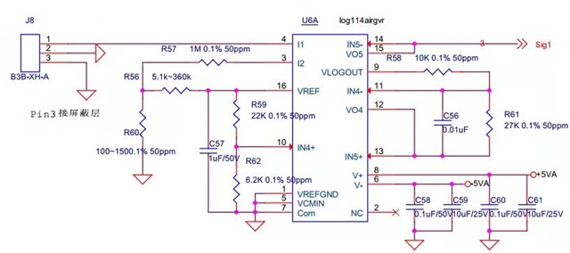
The overall circuit appears to follow the correct configuration similar to Figure 2 on the LOG114 datasheet. The LOG114EVM / datasheet examples suggest bypass capacitors for the V+/V- supplies but do not include a REF bypass capacitor. One potential concern may be stability due to the large bypass capacitor on VREF of 1μF. I will review in the device documentation to see if there are any concerns due to reference stability on my side; but we could consider removing since it is not required.
If you would like me to verify the passive resistors component values, please let me know what is the minimum/maximum current range of I1 required in this application. Also, let me know the required output voltage range requirement for signal 'Sig1". This will allow us to ensure the gain and offset of amplifier A4 is also configured properly.