This thread has been locked.

If you have a related question, please click the "Ask a related question" button in the top right corner. The newly created question will be automatically linked to this question.

TLV9102: driving really large capacitances

Part Number: TLV9102
Other Parts Discussed in Thread: TINA-TI, , TLV9152, REF3425-EP, OPA2350, OPA350, OPA2328, OPA2613, LM8272

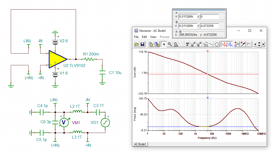
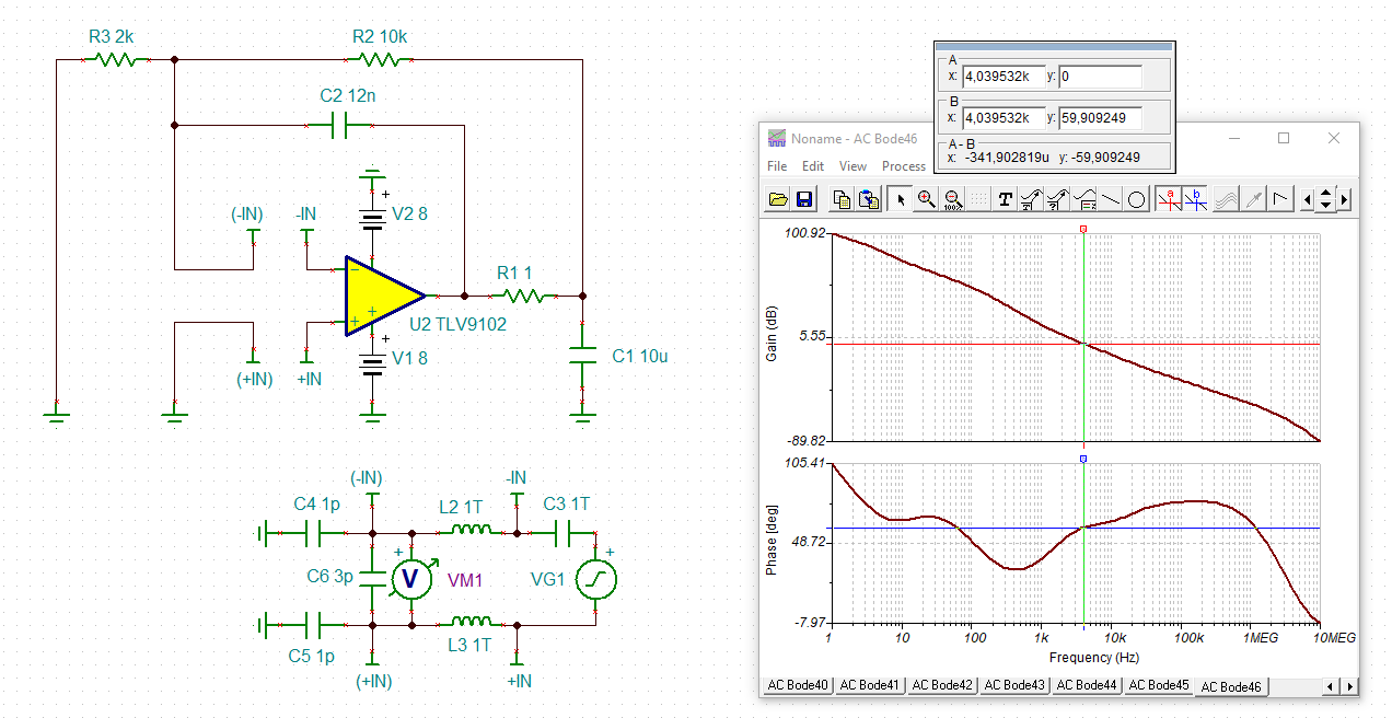
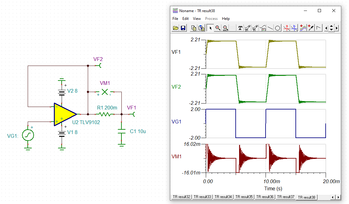
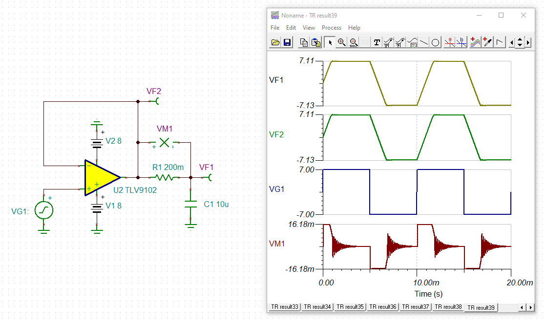
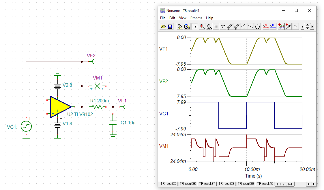
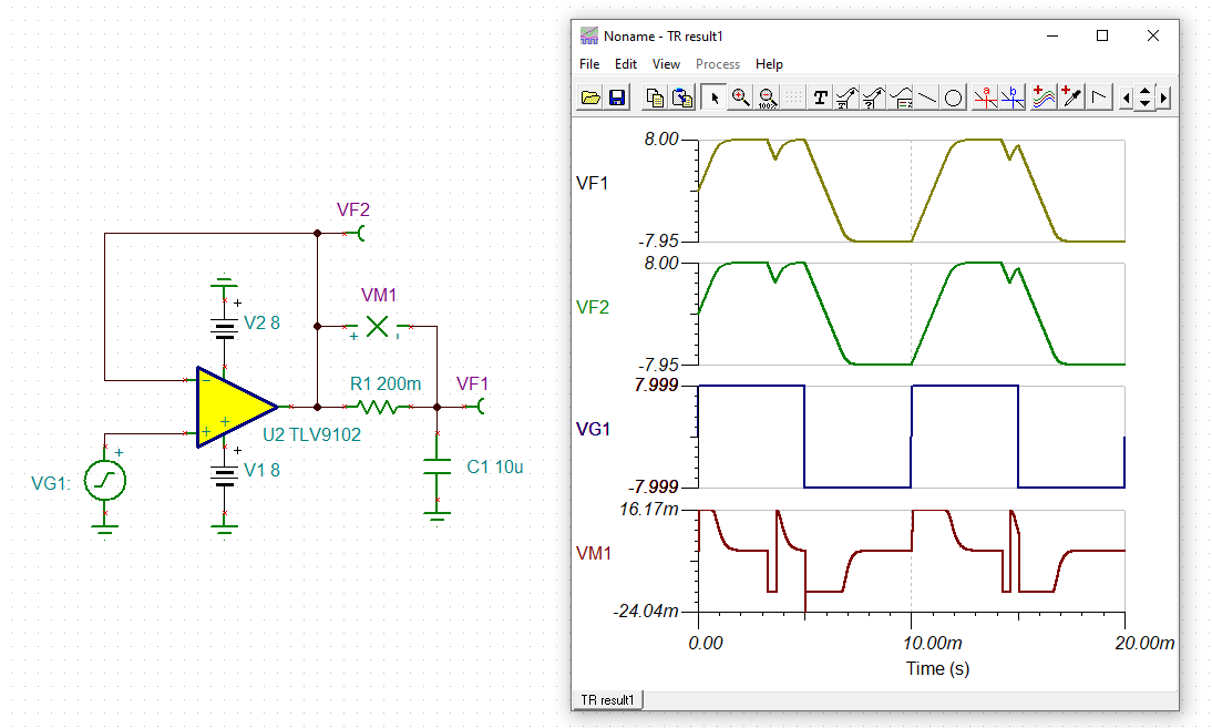
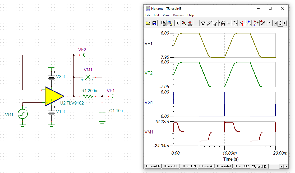
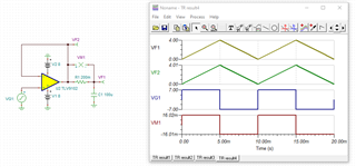
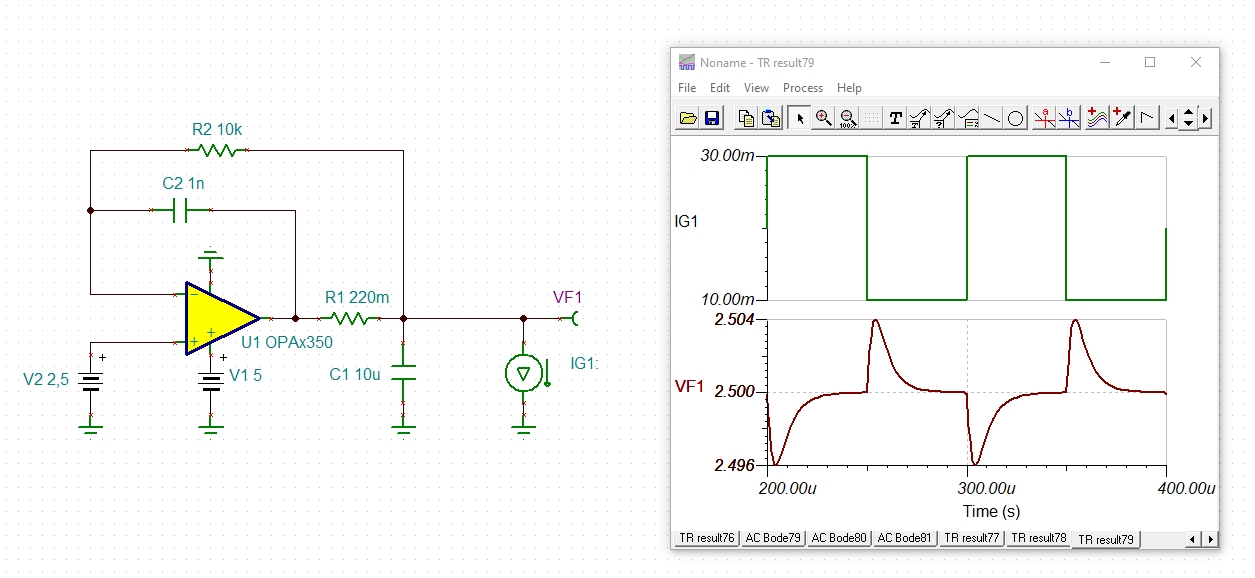
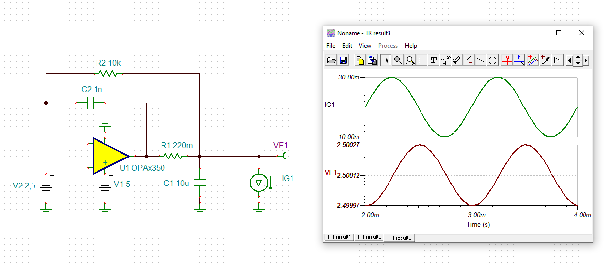
What is the behavior of this OP if it will be used driving a really large capacitance. I’m thinking about 10 µF (or even larger). If there is an isolation resistor between OP output and the capacitor of 0.2 Ohms, I will get a RC time constant of 2 µs. This time constant for loading or disloading the RC combination will be greater than the overload recovery time, listed in the data sheet with 600 ns = 0,6 µs. The OP will be used as 1:1 voltage follower (gain = +1).

Therefore, I would expect that this OP will go into saturation, driving the maximum possible output current and the voltage at the capacitor will go into the desired direction.
Then, if the voltage of the capacitor is close to the final value, the voltage difference between the input pins of the OP will get smaller and the OP will come out of saturation, reducing the output current. Now the OP will regulate the output current according to the residual voltage difference, and the output signal will settle, without any ringing, at the nominal output voltage.

Is this assumption correct?

Or, are there any additional effects causing the OP to start ringing which never ends?

  • Hi User,

    the huge capacitive load will destabilize the OPAmp. See the very small phase margin of only 5°:

    user_tlv9102.TSC

    Kai

  • Once again Kai beat me to the answer! Hahaha

    Hi user1505382,

    Kai is correct. That 10uF is going to destabilize the op-amp. What Kai's showing is how we run stability analysis in Tina-TI, which allows us to better design a circuit that will perform the desired output! In a way this allows us to, in theory, not have to guess what's happening by looking at the transient domain. 

    If you want to learn more about stability and how to run stability analysis, please take a look at our TI precision Lab videos on Op-Amp Stability

    Best Regards,

    Robert Clifton 

  • Sorry, Robert Relaxed

    The phase margin could be improved by increasing the isolation resistor a bit, using dual feedback method and running the TLV9102 at a gain higher than unity:

    user_tlv9102_1.TSC

    Kai

  • Thank you for your answer (which was immediately confirmed by the second amplifier guru).

    Your explanation seem to be the standard behavior of any OP, i.e that behavior would be normally expected. Most OP will go more and more instable if the capacitance at the output is increased.

    .

    But, my question goes above of this behavior.

    I’m not discussing the normal linear operation mode of this amplifier. My question is about the behavior of this OP during saturation and how fast the saturation recovery time will be.

    To my understanding, there should be another curve for any OP, which is only valid for really large capacitances. If the capacitance at the output is very large, than the output stage of the OP will go into saturation – therefore no ringing during this signal slope. During this time there will be a constant voltage drop over the isolation resistor. And due to the limited output current of the OP the voltage at the output of the OP, which is the voltage at the input of the isolation resistor will be lower than the voltage at the +In of the OP. è This is the reason for the saturation.

    Then, if the voltage in the capacitance closes up to the final voltage, the current in the isolation resistor will decrease. Therefore, the voltage at the input of the isolation resistor will no longer be forced by the voltage in the capacitor and the maximum output current of the OP. At this time the voltage between the output of the OP and the input of the isolation resistor will be stable at the nominal setting voltage for the capacitance. And for an OP used as voltage-follower the signal at the –Input will reach the nominal voltage value, too.

    Now, there should be the question, which of both possibilities happen to be faster?

    It the saturation current continues for a longer time, than the voltage at the capacitance will be loaded to a voltage higher than commanded, resulting in an inverse output voltage of the OP and some dis-charging current and this OP will start ringing.

    Or, if the OP will recover faster from its saturation condition, reducing the output voltage and settle the signal to the commanded output voltage without any ringing.

    So far – to my understanding – the relation would be:

    Time-constant of output filter = RC (R_iso x C_load) > Saturation recovery time     ===>   this should result in a stable system.

    Saturation recovery time > R_iso x C_load ===>   This should result in an instable system, since the OP will overdrive the capacitor upwards and then downwards and then upwards and …

    Therfore, there are the following questions:

    1. What is wrong with my expectations of the system behavior?
    2. Why was this behavior not visible in your simulation?
    3. What would be the saturation recovery time of the TLV9152S
      The overload recovery time is listed on page 12 of the data sheet to be 0.4 µs (But with some other test conditions).
    4. If this combination of 0.2 Ohm & 10 µF (Tau = RC = 2 µs) will not result in a stable function, can I receive a stable behavior by increasing the capacitance by a factor 2, i.e. 0.2 Ohm & 20 µF = 4 µs (= 10 times the stated overload recovery time).

    It is very clear, that under this kind of misuse the amplifier will not work with the specified GBW, since it will be mainly dominated by the saturation behavior. But to adjust just one stable reference voltage ….  (Only one stabilization necessary after power-on, or after start of enable-mode.)


    And with respect to the stated GBW, I would expect this to be applicable for a very limited voltage range, given by R_iso x I_out_max. In my example 0.2 Ohm x 50 mA (specified value 75 mA typical) = 10 mV. This should be sufficient, too, since I’m not expecting, that my reference voltage would show greater fluctuations.


    Now, I’m waiting again of your answer, since even this kind of strange application should not be really new to you.


    With kind regards

    Hans-Ludwig

  • Guten Abend Hans-Ludwig,

    as I mentioned, the circuit isn't stable. So it will oscillate when non-saturating and when being driven into light and medium saturation:

    Only when being driven into hard saturation the output will not oscillate:

    user_tlv9102_2.TSC

    But what shall be the benefit of a circuit which can only be driven from hard saturation into hard saturation? It's like driving a car alternatingly with full speed into the front wall and the rear wall. Hhm, that's not what a normal car is being designed for Relaxed

    Kai

  • Guten Abend Kai,

    thank you for your analysis and simulation.

    I will have to think about for a while.

    Just to answer your last statement, your analogy with the car. 
    You are right, that this is not what I’m willing to build.

    What is my interest is more something like:
    A car which is not too fast, but can be driven with full acceleration (or full speed) by pressing the accelerator pedal down to the limit. ( Like an operation amplifier, able to withstand saturation for unlimited time. This is stated in the Abs.Max.Ratings for the TLV9152.]
    With this condition, I’m hoping to come closer to my destination in the shortest time. [= Time interval during which the OP delivers his maximum output current to load the large capacitance]
    Then in the local destination the car should come out of full speed and should approach the target destination quite slowly, limited by the small short-time acceleration due to the small motor in respect of the heavy load.
    [This should be the case in the small voltage range of R_iso x I_out_max, where the OP would only see the voltage at the connection to the isolation resistor and not the capacitor behind this resistor.]


    And I’m a little bit worried by the fact, that I know at least some other amplifiers (ok. I have to agree, those are built by some other manufacturer), which really work just as described by me (even documented in their datasheet). I tried to generalize this behavior (relative tor RC and saturation recovery time), but based on your statements it seems that this is just some operation amplifier with extremely well behavior.
    Or – just another idea of mine, it could be that this behavior could be generalized, but the definition and measurement procedure for “saturation recovery time” might be significantly different between different manufacturers of OPs. And with any other definition of the “saturation recovery time” the behavior after leaving the “saturation recovery time” might be different.


    Just one short additional question, or easy task for you.
    What will happen if you increase the value of the capacitor in your simulation by a factor of 10 and/or 100?
    If my understanding about the physical behavior of operational amplifiers is correct, then there should be a size of the capacitor where the amplifier has no other choice than working stable. It will need some longer time to settle, but it should not show any ringing. This longer RC-constant would compensate any possible differences in the definition of “saturation recovery time”.

    KInd regards

    Hans-Ludwig

  • Hi Hans-Ludwig,

    Kai actually attached the simulation file for your convenience!  But I went ahead and ran the simulation by a factor of 10. With an input signal of 2Vpeak: 

    And with an input signal of 7Vpeak:

    Now just because there's no overshoot or oscillation on the signal doesn't mean that this op-amp is "stable". Unless the intention was to design a triangle wave generator, most people wouldn't want to have the output of the signal so distorted. 

    Best Regards,

    Robert Clifton 

  • Hi Robert,

    your simulation is looking real nice.

    No I don't have the intention to build a triangle wave generator, all I want to do is to buffer the output voltage of a 2.5 voltage reference, to be used as reference voltage for several ADCs and also as supply voltages for these ADCs (using the 2 separate amplifiers within this dual-OP).

    Therefore, I'm interested in one (really only one) settling of the output voltage of this amplifier based on a rising input signal of 2.5 V (after switching on the power supply for the reference voltage and the power supply for this OP). No voltage steps with periodically steps of 2 V_pp or 7 V_pp are planned.

    After this switching-on I would like the output voltage to be stable, even if the current drawn of the capacitor is changing between 10 mA and 30 mA. The edges of these changing current will be damped by the large storage capacitance. The resulting voltage drop at the capacitor will be smaller than 4 mV under worst case conditions. These 4 mV at the output of the isolation resistor with 0.2 Ohms would cause a change of the current through this isolation resistor by 20 mA (i.e. the output current of this amplifier will follow the current of the load with some low-pass filtering by the capacitor, and will slowly change from 10 mA to 30 mA like the current needed by the load). This current of max. 30 mA is significantly lower than the maximum output current of the OP, specified with 80 mA (typical). Therefore, I would expect the OP to react quite slowly, but it should remain stable.

    So to finalize this simulation it would be fine, if you could apply a fixed voltage of 2.5 V as +Input, and an output load with is changing slowly and with very limited voltage difference.


    And it would be really a fine application for this OP. And this would result in a design using only a very small area (WSON-housing with 2.00 mm x 2,00 mm for 2 amplifiers; for the application as voltage follower no external feedback resistors would be necessary [additionally IN- and Out are neighboring contacts], no R_g either) and I would have two stabilized voltage which will not affect the voltage reference since the common mode input impedance of these amplifiers is 6 Tera-Ohm.  

  • Additional Information:

    Typical voltage references like the REF3425-EP needs more space and will deliver only one output current up to 10 mA.

    With my design proposed above I would get 2 additional outputs with up to 80 mA each.

    Kind regards

    Hans-Ludwig

  • Hallo Hans-Ludwig,

    you can have all this with the OPA2350 and by using the dual feedback method:

    user_tlv9102_3.TSC

    user_tlv9102_4.TSC

    Kai

  • Hallo Kai,

    now your proposal comes very close to my requirements.

    However, the smallest housing of the OPA2350 is much larger than that of the TLV9102.

    OPA2350 in MSOP (8) has a nominal body size = 3,00 mm x 3,00 mm, but with the extruding legs the space needed on the printed wiring board is 3,20 mm X 6,0 mm = 19,20 mm² (as given in the land pattern data for the DGK housing.

    TLV9102 in WSON (8) has a nominal body size = 2,00 mm x 2,00 mm, and no extruding legs, therefore the requested space on the printed wiring board is only 2,2 mm x 2,5 mm = 5,50 mm².

    You can see that the OPA2350 needs about 3.5 times the space of the small TLV9102.

    In addition to that, the OPA2350 seems to need some additional components in its feedback loop (one resistor and one capacitor) to deliver a stable signal. These parts might be necessary since the Figure 21 of the datasheet (OPA350, OPA2350 ..) demonstrates that this OP will deliver a non-increasing overshoot for capacitance values greater 10 nF, but it did not show any decrease.
    And these additional parts (even small ones in size 0402) will need some additional space.

    One other part mentioned on the web-site for the OPA2350 which may show some improvements is the OPA2328, whose datasheet shows on figure 6-22 some decreasing overshoots for capacitance values approaching 1 nF (with gain = +1, i.e. operating as voltage buffer).
    And this OP will be available in smaller housings, too. WSON (8) with 3,00 mm x 3,00 mm (without external legs). But this option will be available in some future times, the information w.r.t. this device is preliminary only, and the first prototypes are housed in VSSOP (8) with external legs.


    And I have found another amplifier from TI which seems to fit “nearly” into my design: OPA2613.
    The figure in the datasheet (bottom left on page 9) indicates a decreasing isolation resistor for increasing capacitive loads greater 20 pf. However, the plot stops at 1 nF. With a capacitance of 1 µF to 10 µF the requested isolation resistor might be significantly below 1 Ohm.

    However, this part is even larger: SOIC with 4,9mm x 6,0 mm housing and necessary space on the PWB of 5,1 mm x 7,1 mm and it need quite a lot of quiescent current : 9,4 mA.
    Therefore, this part could not be used, too.

    Kind regards,

    Hans-Ludwig

  • Hi Hans-Ludwig,

    If it wasn't for the package size requirement I would have recommended the LM8272, which has a unique topology to be able to handle driving large capacitors and having minimum external feedback circuitry. I know you are wanting a WSON but would a VSSOP (4.9mm x 3mm) be small enough housing? 

    It would have the advantage of possibly not needing the needed external circuitry to drive the capacitor compared to other devices with a smaller package. 

    Best Regards,

    Robert Clifton 

  • Thank you all, I learned a lot.

    And I have to re-think w.r.t. my design again.

    Kind regards

    H.-L Reischmann

  • Viel Glück, Hans-Ludwig Relaxed