A related question is a question created from another question. When the related question is created, it will be automatically linked to the original question.
If you have a related question, please click the "Ask a related question" button in the top right corner. The newly created question will be automatically linked to this question.
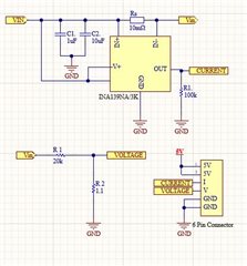
Our customer will use INA139 to read voltage and current values. The input voltage is 7- 28V. The circuit schematic is as shown. Is there any missing or problem in the circuit?
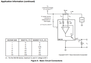
The schematic of the INA139 itself looks fine. As shown in figure 9, V+ can be common or independent of the load supply, so this configuration is ok.
The issue I do see here is with how they have configured the output to their 6 pin connector. They have placed a 1.1Ω resistor between voltage and GND, which, in conjunction with the 20k in series from the INA139 output is most likely going to completely collapse the signal. Note that while the INA139 is a current output device, R1 (100k) will transduce the signal back to a voltage signal, which will then be acted on by this divider. They may want to revisit their calculations on how this signal is passed to the connector.
Our customer got the 100k value based on the data in the table here. Does it cause any trouble? Wouldn't it be right to directly give the output of INA139 from the 6 pin connector part to the 6 pin connector? They want to get an INA139 current output, do they need to remove the resistor in the out (R1)part?
The 100k is fine as they have designed it. My comments above are in reference to the 20k and 1.1ohm. The output at the OUT pin off the INA139 will be gained as per the formula of the datasheet.
Another thought here is that it may be more advantageous though to send the current signal to the connector and place the 100k resistor on the terminating side of the connector, as they would reap the benefits of not having a voltage signal in the cable which is susceptible to noise and dropoff due to trace/cable resistance.
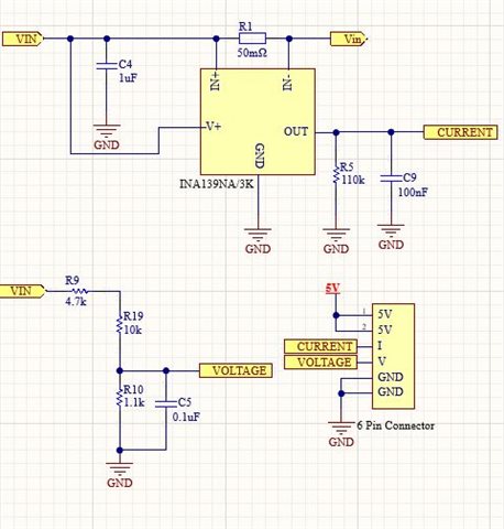
This schematic looks fine. They've stepped up their gain a bit on the output of the INA139 (larger output resistor, and also a larger shunt), and the VOLTAGE signal looks to be a more appropriate division value of VIN (about 1/16th). Some observations for this iteration:
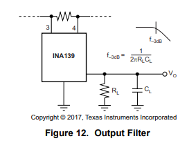
- They have added a 100nF capacitor to the output of the INA139. This is fine for this device, but just make sure they are aware that this will also set a low pass filter for this device, as shown in the excerpt from the datasheet below. For this configuration, their current cutoff is designed at 14.5Hz, so their output will be almost purely DC:
- In the first schematic iteration, they were sending "Vin," whereas here they have changed the signal to "VIN". The only difference between these two is the burden voltage of the sense resistor, so this is most likely not an issue, but I thought I would point this out.