Dear Ti Expert,
I am using OPA2197 (Vs=5V -Single supply ) for my application and calculating worst case offset voltage due to PSRR
below is the snapshot of the OPA2197 and highlighted parameter I am using for calculating offset voltage due to PSRR
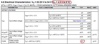
Offset Voltage due to PSRR=( 8V-5V)*2=6 uV where 8V= maximum supply for the given PSRR specification
5V= Application Supply Voltage for OPA2197
Is my approach correct?
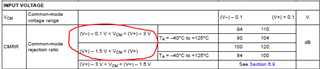
2. My second question is while calculating offset voltage due to CMRR which CMRR specification should I consider ?
below is the snapshot of OPA2197 datasheet.