A related question is a question created from another question. When the related question is created, it will be automatically linked to the original question.
If you have a related question, please click the "Ask a related question" button in the top right corner. The newly created question will be automatically linked to this question.
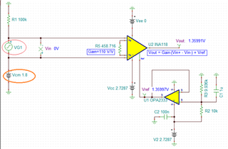
what is the reason for giving the VCM 1.8V in the simulaion
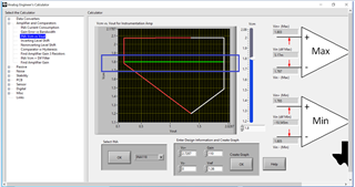
For a give single supply rail, gains and Vref voltage 1.36Vdc), Vcm is centered in the plot of Vcm vs. Vout plot, where small ECG signal is able to maximize the Vout voltage swing. You may choose other Vcm options, if an application is only required to swing within a specific Vout range. For instance, if Vcm is chosen at 1.4Vdc, then Vout's linear response is only able to swing from approx. 0.9V to 1.75 V under the same configuration.
Enclosed is the link of the TI's Analog Engineer's Calculator, you may download it for free.
to prevent us from guessing please show a concrete schematic and refer your questions to this schematic
A suited common mode voltage can be provided by the right leg electrode method. This might be a good idea for an ECG amplifier but not necessarily for an EEG amplifier. It depends on the chosen EEG measuring scheme and there's no simple answer.
A better way is to use a bipolar supply voltage. This would avoid the introduce of a bigger, non-zero common mode voltage.
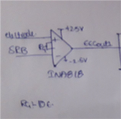
I am capturing the EEG data for that i am using the preamplification circuit which consists of the Instrumentation amplifier stage, 2nd order high pass and low pass Butterworth filter. Below i am attaching the Circuit . when i am simulating the without the VCM i am getting the noise signal.
Could you please help in getting out of this problem
Can you reload a higher resolution schematic in INA818? I am unable to make out the some of contents, including the IA's gains.
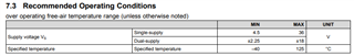
From your image, V+ = +2.5V and V- = -1.6V, and INA818 will require Vs = V+ - V- = 4.1V < 4.5Vdc, which 4.5Vdc delta supply rails are the minimum requirements.
when i am simulating the without the VCM i am getting the noise signal.
when i am simulating the without the VCM i am getting the noise signal.
Could you share the noise simulation plot with us? I'd like to know what part noise signals you are having issues with.
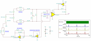
Below is an example of ECG simulation. It was using INA826 and I changed it to INA118 IA, since you are using it. There are similarities between ECG and EEG measurement, and you may get some design ideas from the design approach.
I have used the 5000 gain of the INA amplifier, So i have set the RG value to 10E
I do not recommend to gain up the EEG's application with 5000V/V in a single stage. You may consider to gain up most of input signal gains in the first stage of IA, and make up the remaining gains on the second op amp stage.
INA848 has a fixed gain of 2000 V/V, which it may be suited for your application. The minimum supply voltages are slightly higher than INA118 or INA818, but it has very high CMRR, which is required in your application. If you are able to find INA848 in stock, you should check it out. You may balance the remaining gains with a second precision op amp stage.
If you have additional questions, please let us know.
If you read the op amps' datasheet, you will see that the selection of components are low power, low noise, low voltage, low offset, low drift and RRIO types.
RLD circuit is to sense the common mode noise at IA, then buffer the noise --> invert and gain-up the noise --> add to the RLD location of a patient. The objectives are cancel 50/60Hz and converter it to common mode noise, which it may be rejected by INA118 at the input because of high CMRR.