This thread has been locked.

If you have a related question, please click the "Ask a related question" button in the top right corner. The newly created question will be automatically linked to this question.

OPA858DSGEVM: Max possible amplification

Part Number: OPA858DSGEVM
Other Parts Discussed in Thread: OPA858

Hi there,

This may seem like a simple question, but I was wondering if you would be able to indicate what the maximum possible amplification on the OPA858 is. I have it configured to provide an amplification of 10x, but I have been asked to go as high as 100x. I went over the datasheet and either it wasn't mentioned, or I missed it.

Thank you

Best regards,

Twahidi

  • Hy Twahidi,

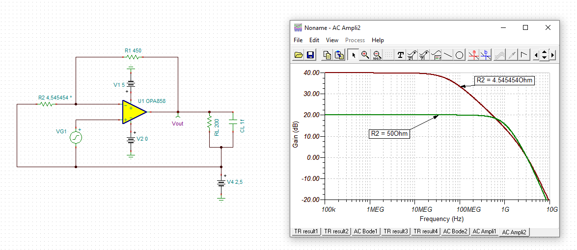
    higher gains are possible, at the cost of lower bandwidth:

     tayeb_opa858.TSC

    Kai

  • Hi Kai, 

    Thank you very much for quick response.

    Essentially I was hoping to amplify an input signal of 60uV ac by around 100x, if not more @ approximately 40MHz. The ideal power supply would be to use dual supply +/-2.6V, though if single supply is preferred that can work as well.

    I had a few questions with the schematic above.

    Is V4 a possible DC replacement for VG1 as the input signal or does is serve a different purpose?

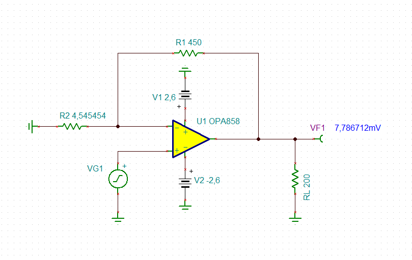
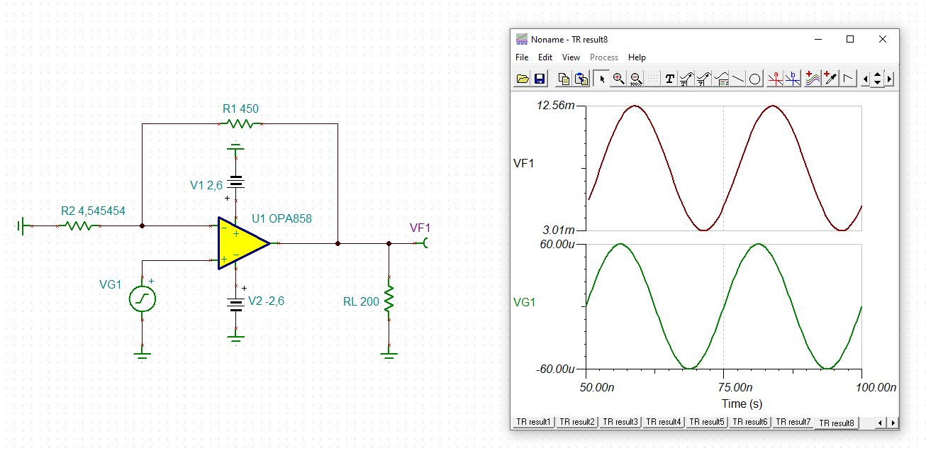
    I have the below configuration setup to amplify an input signal of 60u. I have an OPA858 eval board to test out the validity of the layout but I was wondering if you could give me your opinion on the few alterations I made.

    When I measure the output voltage via the AC Analysis <Calculate Nodal Voltage> I get 13 mV

    When I measure the output voltage via the Transient Analysis  I get 1V output

    Admittedly even 13 mV is a good output (higher is always better), but based on the gain diagram, it should be an amplification of roughly 100x

    tayeb_opa858(1).TSC

    I apologize for the possible overload of information, but any help with the layout would be greatly appreciated.

    Best regards,

    Twahidi

  • Hi Twahidi,

    Is V4 a possible DC replacement for VG1 as the input signal or does is serve a different purpose?

    V4 is from the TI reference design which I adopted because I was in a hurry. Of course, you don't need V4 at all and you can easily power the OPAmp by a bipolar supply voltage.

    When I measure the output voltage via the AC Analysis <Calculate Nodal Voltage> I get 13 mV

    This was the DC offset voltage at the output.

    I have modified the schematic a bit:

    tayeb_opa858_1.TSC

    Keep in mind that the input offset voltage of OPA858 can be up to +/-5mV. So, with a gain of 100 you will see an output offset voltage of up to +/-500mV being superimposed to the wished output signal. You may want to add a high pass filter at the output of OPA858 to remove this DC offset voltage?

    Where is your input signal coming from? What is the source impedance? Is it a sine wave as in my simulation?

    Kai

  • Hi Kai

    The signal source is a photodiode and the source impedance is approximately 50 ohms (SMA connector) and yes the sine wave is correct.

    Thanks

    Twahidi

  • Hi Kai

    I was trying to set up a HPF for the 100x amplifier layout, but the best I got was approximately 30 degrees (though that may be due to my own limitations)

    I decided to  aim for a lower amplification in the hopes of finding a balance between reasonable output and minimal phase shift.

    Based off the ratio between input and feedback resistance, the amplification of the below schematic should be around 30x, yet surprisingly I get almost 100x amplification regardless ( 60uV - 4.54mV) with a phase shift of only 12 degrees.

    tayeb_opa858_0427-4.TSC

    I am going to tryout the layout on my eval board and see how similar the results are to the simulator.

    Best regards,

    Twahidi

  • Hi Twahidi,

    photodiode signals are usually amplified with a TIA (Trans-Impedance Amplifier), as shown in section 10.1 of datasheet of OPA858.

    Kai

  • Hi Kai,

    Hyp TIA amplifier.pdf

    The above schematic is the TIA that was used on our custom board-I am not sure how well it was tested prior to final PCB setup-so it is essentially what I was given to test and try to solve.

    Based off the datasheet the photodiode signal is to the negative input of the opa858 followed by a voltage generator signal to the positive input of the OPA858. I was wondering if you could give me an idea why there would be 2 inputs and whether that was a requirement-or optional.\

    Also if the TIA performs better when using single supply over dual supply.

    Also in theory, how one would emulate the photodiode on TINA

    tayeb_opa858_0427-4(1).TSC

    The phase shift is about 180, but I am assuming that it would be related to the negative input.

    Admittedly I should have specified that the goal was to use the OPa858 as a TIA from the beginning-I apologize for the confusion.

    Thank you once again,

    Tayeb