This thread has been locked.

If you have a related question, please click the "Ask a related question" button in the top right corner. The newly created question will be automatically linked to this question.

INA849: INA849 output is severely offset

Part Number: INA849
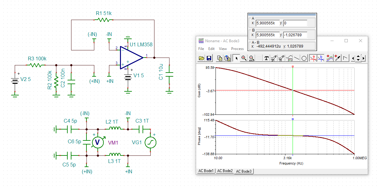
Other Parts Discussed in Thread: LM358, REF4132

With Vref 2.5V, the output should normally fluctuate up and down with 2.5V as the center.

Now the bad problem: when the input is below 4mV, the output is centered at 2.5V,

The larger the input amplitude is, the more obvious the output shift is. When the input reaches 10mV, the shift is about 1V.

Please help analyze the possible reasons and design instructions for related problems.

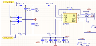
Input differential mode Common mode and power supply are within Diamond Plot safe range

 power supply :+/-10V

  • Hi Sunm,

    please give us a schematic.

    Kai

  • Hi Sunm,

    hmm, the schematic does not show how you drive the REF pin of INA849. According to section 9.1.1 of datasheet the REF pin must be driven very low ohmically, best by the output of an OPAmp. Have you?

    Another question: According to section 9.1.2 of datasheet you must must provide a path to signal ground for the input bias currents. Have you?

    Kai

  • REF drive circuit:

    About signal ground for the input bias currents:

    Trying to connect 1M resistor in parallel for C56 and C62 did not improve the bad phenomenon

  • Hi Sunm,

    Can you remove the caps from the outputs of LM358? They could cause stability issues.

    And make R211=R215=0Ohm.

    Kai

  • Hi Sunm,

    Here are some of schematic suggestions. 

    INA849 E2E 04272022.TSC

    Orange block:

    As Kai pointed out, please remove capacitors at output of LM358, which capacitive loads at output of op amp may lead to loop instability. 

    Red block:

    Differential and common mode LPF may be configured as the reference below. The common mode should be placed at a decade higher than the differential mode LPFs. The reasons are to minimize converting common mode noises to differential mode signals due to tolerances of capacitors. In addition, it will be better to use X2Y capacitor for the part of filter design, since the input impedances should be welll matched in order to reduce CM noises being converted to DM signal.    

     https://www.mouser.com/catalog/specsheets/johanson_johas00924-1.pdf

    Turquoise color block:

    In INA849, the design uses dual power supply rail, so the input Vcm bias may be placed near GND. At its output, Vref2 is configured at 2.5Vdc, which it is you choice. You may a;sp connect to Vref directly to ground since you implemented dual supply rails, see the transfer function in the simulation.  

    The output INA849 is capacitive coupled in HPF and tied to 2.5Vdc at Vref2 voltage. I do not know your intent here. Between Vref voltage and capacitive coupled output, they are some redundancy in the design. Please check it out with the simulation.

    Now the bad problem: when the input is below 4mV, the output is centered at 2.5V

    This is caused by Vout, which is tied to Vref2 (2.5Vdc) after HPF at the output, see the above explanation. 

    If you have additional questions, please let us know. 

    Best,

    Raymond 

  • HI,

    Remove capacitors at output of LM358 is not a good idear,because Vref provides reference for more than 16 ICs。

    After removing, there will be unstable problems such as reference level glitches。

    R72 is connected to VREF2.5V, which is for the convenience of single-power ADC conversion later

    We have initially solved the bad problem now, because there is a large DC difference in the differential output.

    Our project is for EEG applications, if you have a relevant reference circuit, please provide us with a 50HZ 60HZ circuit for reference。

    TKS

  • Hi Sunm,

    the LM358 has lost all its phase margin and is instable:

    sunm_lm358.TSC

    Kai

  • Hi Suum,

    Remove capacitors at output of LM358 is not a good idear,because Vref provides reference for more than 16 ICs。

    Kai demonstrated the instability part of LM358 reference voltage, when op amp's output is driving a capacitive load directly. 

    If a Vref is required to drive multiple reference signals, it is recommended to use bandgap reference voltage ICs, such as REF31xx, REF4132, REF50xx or REF60xx. These reference ICs are capable to source or sink multiple load without suffering stability issues, temperature drift and accuracy and precision degradation etc.. When Vref voltage is driving more than 16 ICs, it is good ideas to partition the signal into 2 or 3 bandgap references on a PCB layout (depending on your application and Vref accuracy), so that the Vref layout signals are not distributed all over a PCB and pick up unwanted noises and transient events. 

    Below are ECG and EEG application reference designs. Some of schematic may not be exactly what you are looking for, but the EEG or ECG analog front end of sensing are very similar or identical in some cases.  


    https://www.ti.com/lit/ug/slau443b/slau443b.pdf?ts=1651099983934&ref_url=https%253A%252F%252Fwww.google.com%252F

    https://www.ti.com/solution/electrocardiogram-ecg?keyMatch=ECG%20REFERENCE%20DESIGN

    https://www.ti.com/lit/ug/slau443b/slau443b.pdf?ts=1651099983934&ref_url=https%253A%252F%252Fwww.google.com%252F

    https://www.ti.com/lit/ds/symlink/ina826.pdf?ts=1651084895132

    If you have additional questions, please let us know. 

    Best,

    Raymond