Other Parts Discussed in Thread: DRV8300, INA286, INA281, INA240, INA293
Hi,
I'm trying to build a custom motor control board, using a C2000 uC.
As a driver IC, I use the DRV8300 and for current measurement, I use the INA286 (because it is one I could find easly, evertyhing with less than 100V/V gain is really hard to get).
Now, all the signals (Vsupply, Va, Vb, Vc, Ia, Ib, Ic) can be measured, but I noticed, that when I start the controller PWM (without motor at the moment), I immediately get really high noise peaks on the current measurement and I don't really know, how they occur. I was pretty careful with the design, but it seems, that I have done something wrong or that the INA286 with such a low shunt is not handable. I will try to desolder the cap at the differential input, maybe that could be the problem?
There is no noise on the 3.3V supply for the IC, so also this cannot be the source of the noise.
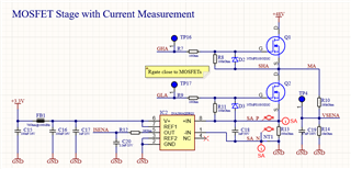
Here is the schematics of phase A with the current measurement path:
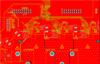
Layout TOP:
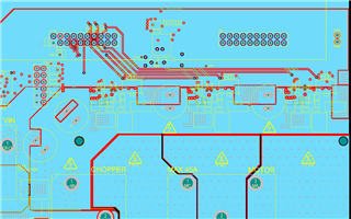
Layout GND:
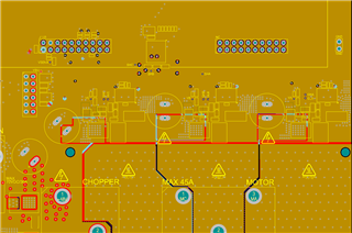
Layout VCC_SIG:
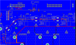
Layout BOT:
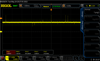
Osci INA286 OUT (huge peak):
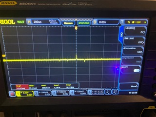
So, can you see something that is really wrong here or is the IC not really dedicated for motor control? There are no peaks on the shunt itself, when I measure the HIGH side of the shunt.
So it really is somehow coupled into the measurement IC.
Edit:
So I also measured the high side shunt and the INA286 output. I could not use a sping probe, thats why you see the PWM signals, but I think that makes the capture more valuable.
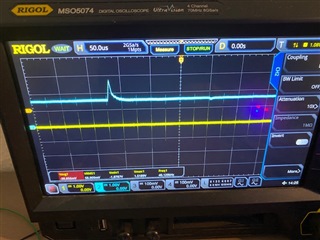
It seems, that the start of such a overshoot is somehow triggered by a PWM signal, I really cannot explain that behaviour
Edit2:
The INA281 has this switching capacitor structure:
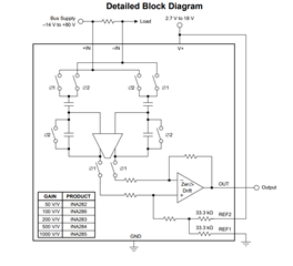
Might this be a problem?
Edit3:
The pulses seem to occur always around 3-4us after a PWM Signal:
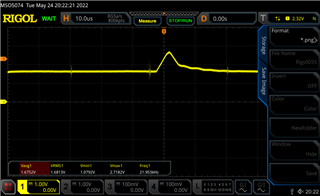
And the pulses seem to be pretty random: