This thread has been locked.

If you have a related question, please click the "Ask a related question" button in the top right corner. The newly created question will be automatically linked to this question.

EMG active amplifier using INA326

Other Parts Discussed in Thread: INA326, ADS1294

Hi,

I am designing an EMG amplifier using the INA326 as the differential input component. I have referred to many of the forum posts involving the design of EMG/ECG amplifiers but still I am unsure about a couple parts of the design.

1) Design for Single Supply

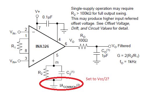
I intend to power the INA326 using Vcc = +5V and Vss = GND. Am I correct that I then must bias reference pin 5 to Vcc/2? Also are there any impedance requirements for pin 5? I plan to derive Vcc/2 using a buffered op-amp configuration for low output impedance.
2) I am using a cascaded low-pass and high-pass filter for the following stage and with the output from the INA326 at Vcc/2 subsequent filter op-amp stages are biased to Vcc/2. I am getting a bit confused in terms of knowing how to handle COM of the patient, GND of the sensor/amplifier board (Vss for INA326 and filtering op-amps) and the reference voltage Vcc/2 that the EMG signal will ride on. Currently I plan to use a driven right leg configuration to set the COM potential of the body to Vcc/2 and provide high common mode rejection for 60 Hz noise. A reference schematic of the setup is included below. I have not optimized the feedback loop of the DRL yet to improve stability. Do I have the basic configuration correct? And is my methodology of driving the body potential to Vcc/2 since it is used as the common of the INA correct?

1004.driven_right_leg_sim.pdf


3) In terms of the INA326 bias currents currently the only path is from ground through the body and through the electrodes. I did not want to provide an additional path to GND (VSS) on the inputs as that would degrade input impedance. Will the output of the INA326 saturate if the electrodes are not connected to the body and bias path is not provided? Or does the driven right leg circuit provide an additional bias path for the INA326? A reference schematic of the INA portion is provided.  Do I need to provide any additional considerations for accommodating the bias currents required by the INA326?

6648.INA_326.pdf


Thanks,

Chris Wiebe

  • Hello Chris,

    I am working on this and will get back with you shortly.


  • Hello Chris,


    Thank you for considering the INA326 for your EMG amplifier.  Here are the answers to your questions:


    1)      Yes, bias Vref to Vcc/2.  Please note that due to the topology of the INA326 you do not necessarily have to have a low-impedance source.  When used in single-supply configuration, be sure to use large values for R2 to ensure that the current flowing into pin 5 remains under 25uA.  Please refer to page 10 and Figure 7 of the PDS.

    2)      The use of the RLD amplifier to bias the common-mode is correct.  It is also used for noise cancellation.  I have attached slides that discuss RLD.

    3)      The RLD circuit provides the bias current path for the INA.  If an electrode becomes disconnected, it is likely that the INA will saturate.


    RLD.pdf
  • Pete;

    If we could find John Brown he would be a great resource for biomedical electronics answers; he wrote a texbook on biomedical instrumentation. Many of the INA circuits were developed by John.

  • Thank you for the help Pete. Preliminary tests showed great results. One thing I did not expect however is that I did not need to drive the body to 2.5V. The INA326 is able to amplify and drive out the differential signal even if the input swings about VSS (GND) for single supply application. I grounded one input and applied a sinewave with zero offset to the other input and increased the amplitude until the output saturated at GND/5V. I see from the datasheet that the tolerable common mode input voltage is VSS - 0.5 to VCC + 0.5. So it makes complete sense that it worked, I am just surprised that the inputs can swing so far below VSS. Is there any other case I am missing for why I should drive the body to 2.5 V (REF of INA) instead of GND?

    Hi Neil, yes if John Brown is available for future reference I would appreciate his opinion as well relating to the question above.


    -Chris

  • Hello Chris,


    Biasing to Vs/2 will allow for maximum common-mode rejection.  There is a discussion on page 65 of the ADS1294/6/8 PDS.  The following forum post also discusses RLD and notes that it is also an accepted standard reference point from which the Vcm is established.

    View this post at http://e2e.ti.com/support/amplifiers/precision_amplifiers/f/14/p/347/1464.aspx#1464

    As noted in the post, depending on your application your overall SNR may be good enough such that you do not need RLD.

    John Brown retired from TI a couple years ago and I have no contact information for him.