This thread has been locked.

If you have a related question, please click the "Ask a related question" button in the top right corner. The newly created question will be automatically linked to this question.

TLV313: Maximum Filter Driving Capabilities

Part Number: ADS1296
Other Parts Discussed in Thread: TLV313, , TINA-TI

Dear Experts,

my application requires a high input impedance. Therefore I am using 2 x TLV313 OpAmps as unity-gain buffers for my ADS1296. They also provide an adequate common-mode output voltage (2.5 V) for my ADC. My signal of interest is 0 - 10 kHz. The ADCs modulator frequency (as I understand is the actual sampling frequency) is, depending on the mode, 512 kHz or 256 kHz, which puts it's Nyquist frequency to 256 kHz or 128 kHz. At and above the Nyquist frequency I would want to have significant attenuation of my input signal to not have components above that frequency folding back into my spectrum of interest.

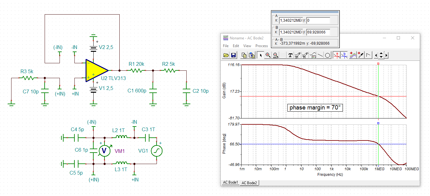
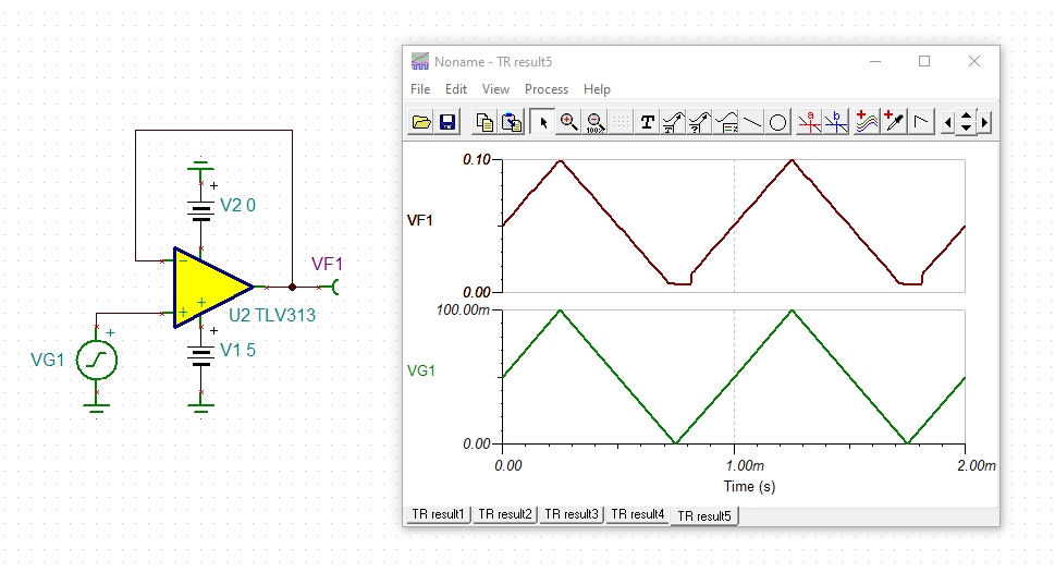
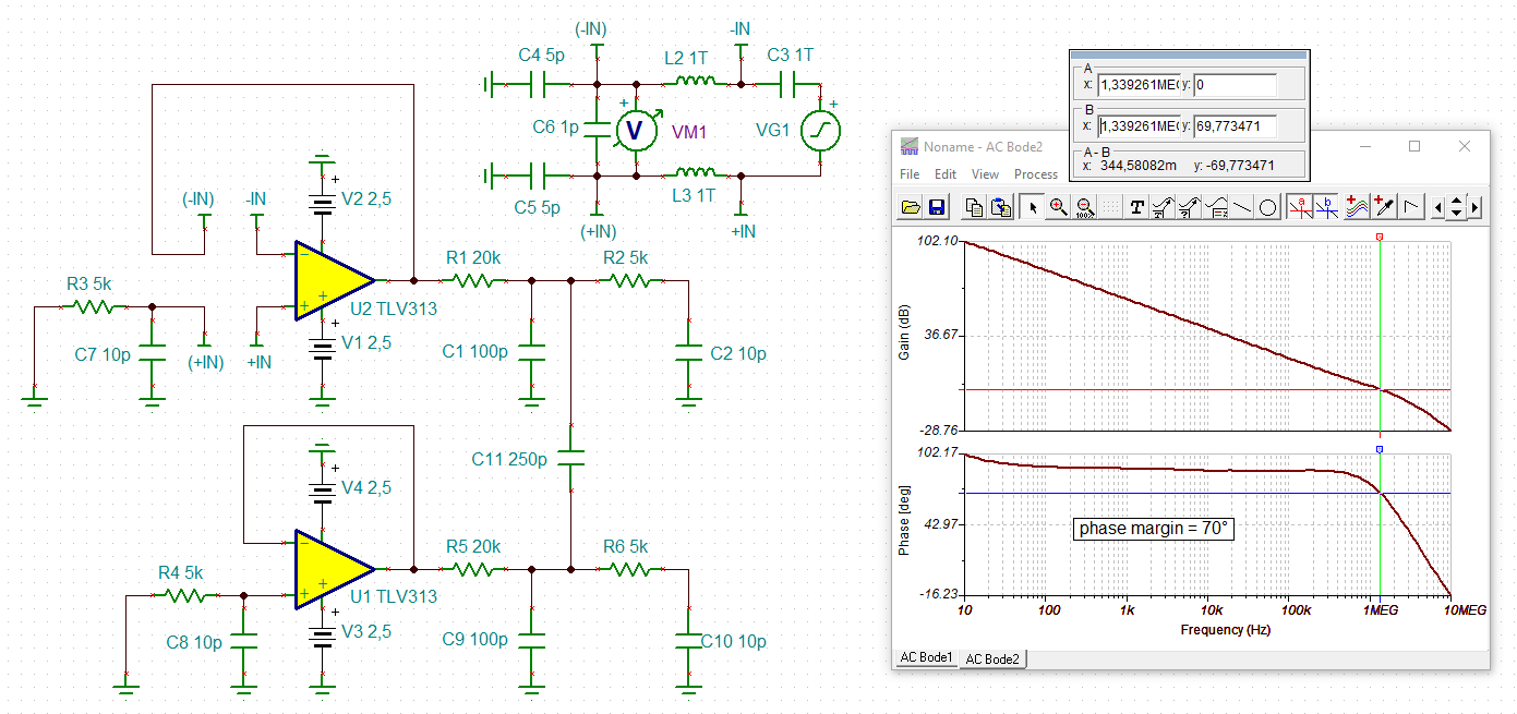
However, I cannot build a reasonable (RC) low-pass at the input of the TLV313, because the capacitor to ground would decrease my input impedance, which I need. E.g., the TLV313 has an input capacitance of 1 pF and an RC low pass with a cutoff frequency of 25 kHz for example, in combination with a 10 kOhm series input resistance of the TLV313 (recommended to decrease input current at a reasonable noise level), would already require a capacitance to GND of 630 pF (and hence strongly decreasing my input impedance). I am willing to build a strong filter (e.g., third order Chebyshev) at my TLV313 output stage. However, I only find that the TLV313 can drive up to 1 nF of a purely capacitive load (TLV313 OpAmps, page 17). How do I know if this works with a more complicated filter inlcuding uH inducatances, uF capacitances and some kOhms?

This is my current design (limited attenuation at 128 kHz --> around 20 dB or so):

So my questions are basically manifold:.

1. How large do I need to filter/attenuate my signals at the Nyquist frequency already?

2. What is the usual/good practice to employ a strong filter after unity-gain buffers?

3. How do I know if my TLV313 will function with a complicated mix of R-L-C in case I use a higher order (Chebyshev) filter? What are the resistance limits for my TLV output/my ADC input? I read with another ADC from Analog that the series resistance towards the ADC cannot be larger than 2 kOhms for example, for the ADC to be able to buffer / get enough current. For this ADC I don't find this information.

4. At a data rate of 32 kHz my noise level is quite high: 521 µV_RMS and 5388 µV_pp (5.4 mV_pp). What is the minimum input signal (sine wave) I require to still be able to have a proper signal? I searched a bit for SNR on different applications but only found very general statements. What should the peak to peak voltage of my input signal be as a minimum?  

5. From the ADS1296 datasheets it reads that the gain does influence my noise. But if my noise is halve the value at twice the gain for example, from my thinking this would not give me much, as I would need to decrease my input signal strength as well. So the SNR is basically the same (e.g.: 2 V input signal and 500 µV_RMS noise at Gain = 1; is equally reasonable than 1 V input signal and 250 µV_RMS noise at Gain = 2). Am I missing something?

Any input is highly appreciated!

Best wishes and thank you! Rene

  • Hi Rene,

    I read with another ADC from Analog that the series resistance towards the ADC cannot be larger than 2 kOhms for example, for the ADC to be able to buffer / get enough current. For this ADC I don't find this information.

    See figure 39 of datasheet. The input bias current of /-200pA at room temperature causes a voltage drop across the input series resistance which adds to the offset voltage of ADC.

    How do I know if my TLV313 will function with a complicated mix of R-L-C in case I use a higher order (Chebyshev) filter?

    By performing a phase stability analysis. But with your high R the TLV313 should be stable.

    Please replace R3 and R4 by short-circuits. This is a CMOS OPAmp with ultra low input bias currents. There's no need for an input bias cancelling scheme. R3 and R4 only destabilize the OPAmp.

    How large do I need to filter/attenuate my signals at the Nyquist frequency already?

    This also depends on how much unwanted noise you have at all. The higher the noise the more filtering you need and vice versa. There's no simple answer. And it's best to check it out with a real circuit.

    Kai

  • Dear Kai,

    really appreciate your feedback to the cirucit! So any OpAmp output should be fine as I understand now the low ADC input bias current requirements. This is nice, so I can build a stronger filter! I will also read into the documents provided by TI concerning phase stability of OpAmps!

    Do you have any feedback on question 4. and 5.? Is my thinking there correct? Any advice or references are greatly appreciated. As a newcomer the biggest issue is to phrase a question right/find the right tags/keywords to look for.

    Thank you once again,

    Rene

  • Hi Rene,

    the best source of information is the datasheet of ADC. Yes, I know, it's hard to read but it contains everything you need.

    To properly read table 3 and 4 of datasheet, first think about what bandwidth you need. Then, think about whether you want to use the internal PGA. What gain do you need in the PGA? The first purpose of the PGA is not to improve the noise, but to deliver the gain you need. Because of that, certain gain settings may offer more or less noise or even the same noise, so that certain gain setting seem to make no sense in improving the noise.

    Kai

  • Hey Kai,

    I don't need the PGA as I can tune my input signal magnitude via my input impedance. And my bandwidth is 10 kHz I think (signal of interest).

    One more question. I looked at this TI tutorial concerning phase margin stability:

    https://www.youtube.com/watch?v=DfrPeUnfZ3U (see 6:57 min)

    and tested it with an exemplary circuit. Working well. However, one questions that remains open for me: in my circuit my Rf = 0 and R1 = infinite (Unity-Gain Buffer). How can I find the phase margin then, as my gain (or Aolβ, or Vo) is below 0 dB all the time; see here:

    I don't find where to look for the intersection of curves as you would check Aolβ crossing 0 dB, normally.

    Thanks, Rene!

  • Hey Rene, 

    You have to right hand click on the curve and select Phase margin: 

    All the best,
    Carolina

  • Hi Rene,

    your input signal is too low and you drive the output into saturation. By this the OPAmp leaves its linear operating range and the simulation will fail. Increase the input voltage so that the output goes out of saturation. Like this, for instance:

    rene_tlv313.TSC

    Kai

  • Hi Kai,

    thanks for the model! Things are clearing up. However, it  is not really clear to me what you mean by "...input signal is too low...". The input (voltage generator) should be the same in our models and is determined by the AC Voltage source used for the frequency sweep automatically, right?

    1. The only difference in our models is that I used single rail supply (+5 V and 0 V) and you used dual rail supply (+- 2.5 V). Why? In my application I want to use the single supply option as I get an output voltage swinging around 2.5 V, which is optimal for the ADC inputs.

    2. How do you come up with the capacitors C4, C5, C6, C7? From experience? I did not see them in the TLV313 datasheet?

    3. Can I directly test the phase margin with the two parallel OpAmps configuration (my initial design) as well? I also plan a capacitor between both OpAmp outputs. If I cannot determine phase margin stability with the dual OpAmps configuration, I would need to integrate this capacitor (between both outputs) in a scaled version (probably halve the value) at the output.

    Again, thank you so much. Really appreciate our valuable conversation and looking forward to your answers!

    Have a good day,

    Rene

  • Hi Rene,

    forcing the input voltage of TLV313 to the negative supply rail (0V for a single supply circuit or -2.5V in my simulation) will drive the output of TLV313 into saturation:

    Or by other words, the output can no longer follow the input voltage. The OPAmp is no longer operating linearily and the feedback loop is out of regulation. -> Your simulation will not work.

    Increase a bit the input voltage so that the output comes out of saturation and everything will be fine.

    C4, C5 and C6 are the input capacitances of TLV313. And C7 is from your schematic.

    To simulate the differential amplifier (U1 and U2 in your schematic) just add the second TLV313. By this the output impedance of second TLV313 is included in the simulation.

    Kai

  • Great Thank you again. Really interesting that you need to model the stray- and input-capacitance explicitely! I always thought they would be represented in the macro model already. And good that you clarified this, otherwise I would have added these additional capacitances on my PCB. =)

    Okay but changing the supply for the frequency sweep makes sense. In my application the input does not get close to the supply (5 and 0 V), thats why I never faced that issue of saturation/non-linearity before.

    I only have one last question: Why do you measure the voltage over the OpAmp inputs instead of the output voltage (as in the TI Tutorial)? In the diff amplifier design there are significant differences, whether I measure the way you did (phase margin 70°) or over the output to GND (7°). See here:


  • Hi Rene,

    you would do it this way:

    rene_tlv313_1.TSC

    C4...C6 are the common mode input capacitances and differential input capacitance of TLV313, which have to be externally connected to the loop with this sort of phase stability analysis. Otherwise the OPAmp output would not see these input capacitances because of the isolating L2 and L3.

    C3, L2 and L3 are just representations of "ideal" caps and "ideal" inductances.

    The idea of the analysis is to stimulate the inputs "IN+" and "IN-" of OPAmp by the help of "VG1" and to look what comes back to the inputs "(IN+)" and "(IN-)". The dampening and the phase between the input signal and the returned signal is used to make the "Open-Loop Gain and Phase vs Frequency" plot and to calculate the phase margin.

    This method I have learned from TI's Mr. Tim Green. It has the advantage that you do not have to work with the TINA-TI's post-processor. It also allows to take into consideration the individual output impedance characteristics of OPAmp.

    Kai

  • Nothing more to add than a huge thanks! Thank you for taking the time to teach and share your experience! Great support forum!

    Have a great week Kai!

  • Thank you and good luck Relaxed

    Kai