This thread has been locked.

If you have a related question, please click the "Ask a related question" button in the top right corner. The newly created question will be automatically linked to this question.

OPA552: Device sometimes break

Part Number: OPA552
Other Parts Discussed in Thread: OPA593, TINA-TI, OPA551

Hi ,

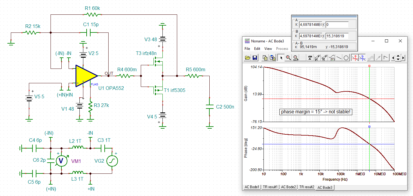
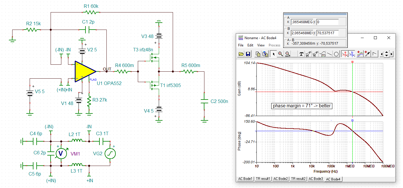
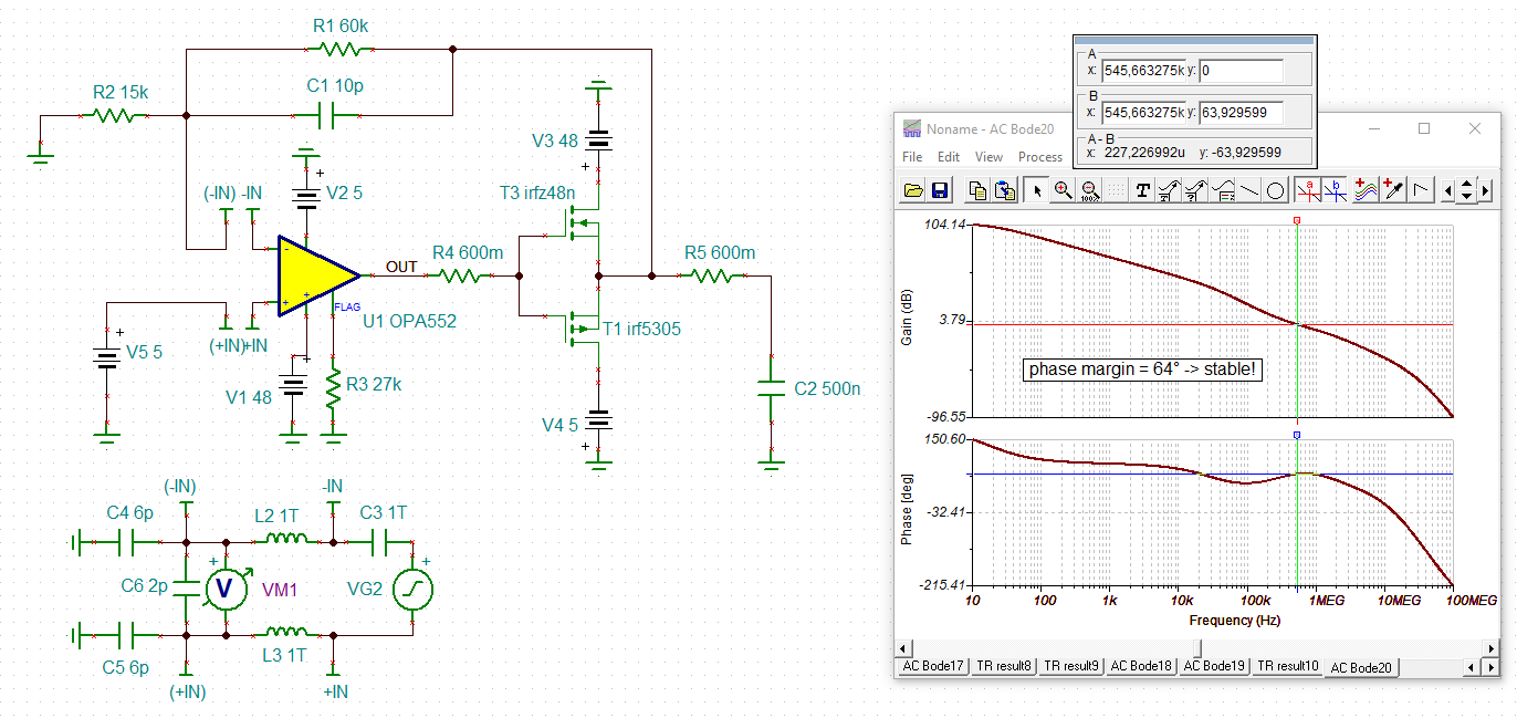
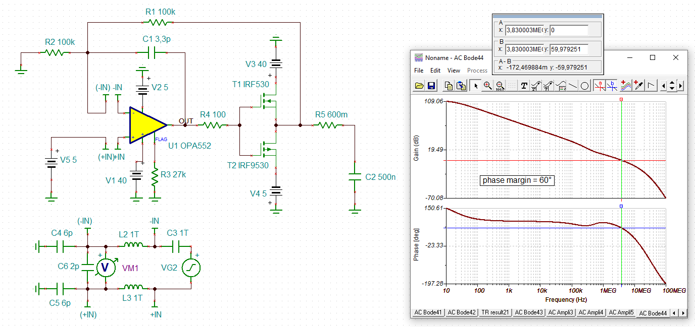
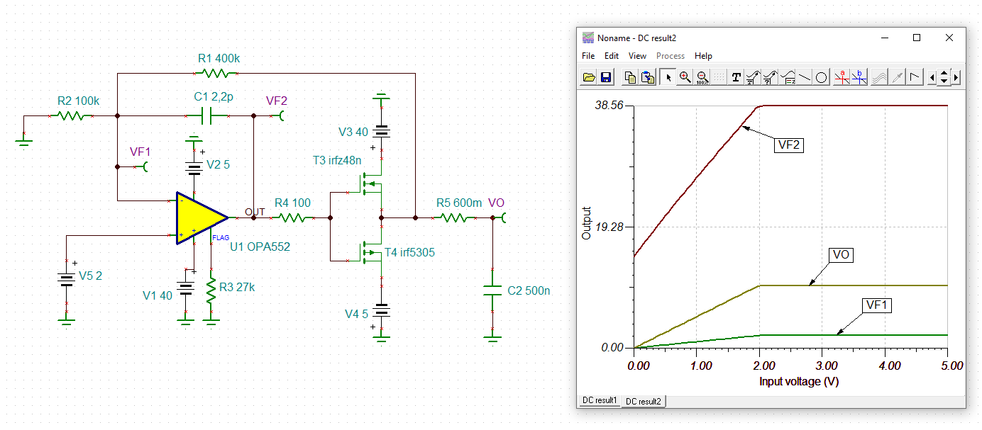
I have been trying to make some circuits to improve the slew rate for the capacitive load from 1nf until 470nf using OPA552 (DDPAK package ). Attached below is the circuit. Some insights of the circuit, the cascaded gain circuit is 5.

When the input is about 7.4volts, the device broke and until 7 volts it was alright. Vs+ = (+44V) and Vs- = (-5V) ---> A PCB was built for same circuit.

update:

Found out that the first opamp in the cascaded circuit was broken.

Please help me with this.

Please let me know if something else is required.

B.R,

Tarun

  • Hi Tarun,

    have you carried out a phase stability analysis?

    Kai

  • Hi Kai,

    I have made some bode plots using ltspice and bode 100, it was fine till 100khz. is it what you were asking. Will check some info online if available also any info from you would also be great.. And also just an update that The first opamp in the sequence was broken.

  • Is this the right way to phase stability for a cascaded system? 
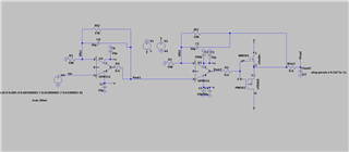
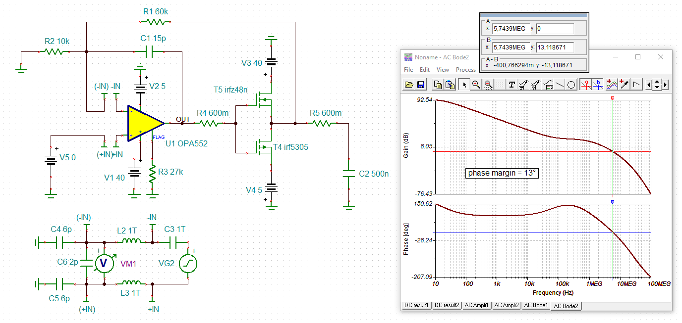
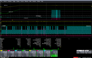
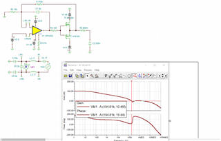
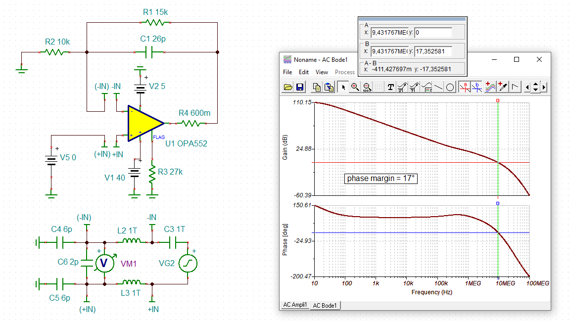
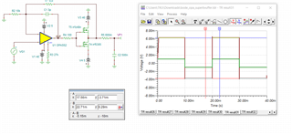
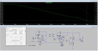
Here is the phase response of the first cascaded circuit.

  • Hi Tarun,

    I would eventually do it this way:

    tarun_opa552_4.TSC

    tarun_opa552_1.TSC

    Kai

  • Hello BR,

    First, thanks to Kai for his extensive stability analyses of your OPA552 applications circuit.

    You mention the OPA552 device "broke." Does that mean that "first" op amp has been damaged in the application circuit and no longer functions? That would not be expected unless something unusual occurred in the circuit. 

    The OPA552 is not a unity-gain stable op amp. It is an undercompensated op amp that is optimized for closed-loop gains of 5 V/V, and greater. Your first stage has a closed-loop gain of 2.5 V/V and the second stage has a closed-loop gain of 2 V/V with the addition of the external MOSFET output buffer. Therefore, there is a high probability of instability in both of these stages unless the added components around the OPA552 op amps happened to produce in a stable condition.

    If an op amp breaks into a high-level oscillation condition what can occur for some devices is the output stage goes into an output current shoot-through condition. When that happens high current shots through from one output transistor to the other. This unusual condition takes place because one output transistor has not had enough time to return to its low current class AB state, before the other transistor has ceased sourcing or sinking current through it. If the current through the transistors is very high they can overheat and be damaged. That is what likely occurred in your circuit.

    Regards, Thomas

    Precision Amplifiers Applications Engineering

  • HI Thomas, yes the opamp in the first stage was no longer functional. any recommendation, for better stability and to drive capacitive loads till 470nf with voltage until 36V. is this current you were taking about?

  • Hi Tarun,

    You mentioned it was the first OPA552 op amp that "broke." The shoot-through current I described could occur with either the first or second OPA552. However, since the first OPA552 is damaged it is the one whose output stage could have conducted an excessively high current resulting in it being damaged. 

    If the OPA552 is operating satisfactorily as an intended linear amplifier and not oscillating the described possibly damaging condition would not occur. 

    Regards, Thomas

    Precision Amplifiers Applications Engineering

  • Hi Tarun,

    Have a look at TI's new OPA593 high-voltage, high-current op amp. It provides a high slew rate of 40 V/µs and is unity-gain stable. The output current capability is typically 250 mA, and it will easily work with your +40 V/-2.5 V supply arrangement. Since your application has the high capacitance drive requirement of 1 nF to 470 nF almost certainly it will require compensation to assure stability. This would be a requirement for nearly any op amp.

    https://www.ti.com/lit/ds/symlink/opa593.pdf

    The OPA593 has a built-in, user settable current limit function. If you attempt to slew too quickly with a high-C load current limiting will be initiated when the set limit is exceeded.

    Regards, Thomas

    Precision Amplifiers Applications Engineering

  • Hi Thomas, thanks for the suggestion. Looks like it's (opa593) not available in online stores.

    with some compensation, techniques like composite amplifier loop and compensation resistor.

    - I am thinking of having a gain of 5 in the first and second stages which gives a 25 gain. do you think it's a good idea?

    - Do you have any other suggestions to compensate or for producing a high slew rate?

    Thanks for you your time.

    B.R,

    Tarun

  • Hi Tarun,

    I would encourage you to carry out a phase stability analysis of your circuit, one for each OPAmp.

    Unfortunately, I was not able to find proper Spice models of your MOSFETs. So I changed them to the IRF530 and IRF9530 which are both known by TINA-TI.

    Thomas is fully right, that the OPA551 is better suited than the OPA552, even if my phase stability analysis showed an acceptable phase margin with the OPA552.

    In the meanwhile I also performed a phase stability amaysis of your first OPA552 and I can say that your circuit is not stable!

    tarun_opa552_3.TSC

    A too low phase margin (< 45°) causes instability and oscillation. And oscillation is very well known to be the cause of damage of an OPAmp, because oscillation can heat up the die until thermal destruction.

    So please carry out a phase stability analysis first, before experimenting with the real circuit. A phase stability analysis can easily be done in LTSpice as well.

    Two additional points:

    1. This dual feedback method to restore the phase margin only works properly for a rather limited range of load capacitance. Watch this very nice TI's training video series on stability:

    https://training.ti.com/node/1138805

    2. Keep in mind that a high slew rate and a high capacitive load are "natural enemies". Because the load current into a capacitive load depends on the change rate of applied voltage -or by other words- the slew rate, according to

    I = C x dU/dt

    an abnormally high slew rate means an abnormally high load current.

    So, as still being a real world circuit, if you don't want to end up with unlimited load current spikes you will need to limit the slew rate somehow, either by introducing a low pass filter at the input of circuit or by taking an OPAmp with a limited slew rate.

    Kai

  • Thanks kai. will work on it and see if I can figure out something.

  • Hi Tarun,

    Regarding your questions:

    - I am thinking of having a gain of 5 in the first and second stages which gives a 25 gain. do you think it's a good idea?

    The OPA552 should be stable in a gain of 5 V/V, and higher such as 25 V/V providing the output load complies with the information provided in Figure 19. The high capacitances you are planning on driving certainly requires additional compensation which Kai has illustrated so well.

    - Do you have any other suggestions to compensate or for producing a high slew rate?

    The slew rate of the OPA552 is internally set by the internal compensation capacitor and the maximum current rate at which it can be charged. The only other real option is a higher slew rate op amp. Unfortunately, I don't have another one to suggest that meets all your circuit requirements.

    Regards, Thomas

    Precision Amplifiers Applications Engineering

  • Hi Tarun,

    I have carried out additional TINA-TI simulations and can say that the circuit with the OPA552 has a stable phase margin of about 59° for all capacitive loads between 1nF and 500nF. The slew rate is about 15V/µs.

    The same circuit with the OPA551 shows a phase margin of about 78° and a slew rate of about 10V/µs.

    Kai

  • Hi Kai,

    It could be great if u could share the circuit or the Tina simulation file about which you are talking about?

    Thanks.

    B.R,

    Tarun

  • Hi Tarun,

    it's exactly the circuit shown above with the MOSFETs.

    Open the

    OPA551 TINA-TI Reference Design (Rev. B)

    copy the model of OPA551 and paste it into my circuit.

    Kai

  • Hi Kai,

    Thanks for the stability analysis videos, now I understand much better what you were talking about. I started doing here some transient analysis using the small signals.

    When I use a square wave as an input I get what I expect as shown in image TI5 but I use the UNIT step as input as shown in IMAGE TI6 when I already have some voltage when the vin is 0, couldn't figure out why?

    And it only happens for small signal nor large signals as shown TI7.

  • Hi Tarun,

    do you mean the input offset voltage of OPAmp? The input offset voltage of OPAmp will cause a small DC shift of output signal. This is fully normal.

    Can you post your TINA-TI simulation file? Use the "Insert" button at the bottom of your input text window.

    Kai

  • Hi Kai,

    alright. Please find it in the attachment. Also I tried to make some loop gain and 1/beta to find phase margin, although the plots look pretty abnormal.tarun_opa552_mosfetUpdate.TSCtarun_opa552_mosfetUpdate_bode.TSC

  • Hi Kai, 

    is this also the right way to find the phase margin? if then, are there other methods except using isolation resistors to compensate the circuit better?

    and also I would thank you for your time as now I much better understand the phase response.

     tarun_opa552_AnalysisBodefinal.TSC

  • Hi Tarun,

    I don't get your MOSFETs to work. Me thinks that there's either a mistake in the very old Spice models (1996 !) of these MOSFETs or that these MOSFETs are not well suited for your circuit. Try to find other, new MOSFETs with a proper Spice model.

    Kai

  • Hi kai,

    í tried to send these models but couldn't in this. So I attached the links here

    https://www.infineon.com/cms/en/product/power/mosfet/n-channel/irfz48n/#!?fileId=5546d462533600a40153572d21533c6f

    https://www.infineon.com/cms/en/product/power/mosfet/p-channel/irf5305/#!?fileId=5546d462533600a4015356fb1fcd36ce

    and these worked for me in tina's simulation too. The attached simulation shows me a phase margin of 78 but with less bandwidth though. Do you think it's stable? or am I doing something wrong.

    5355.tarun_opa552_AnalysisBodefinal.TSC

    Best Regards,

    Tarun Kumar

  • Hi Tarun,

    even very small input voltages drive the output of OPA552 into saturation:

    tarun_opa552_5.TSC

    Kai

  • yeah, i observed the same thing. but with Ltspice, it shows like expected. don't know why it is so.

  • Hi Kai, made some plot usin 
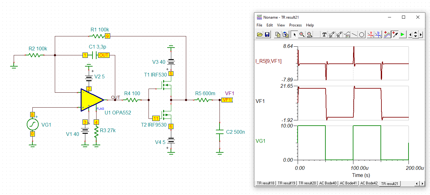
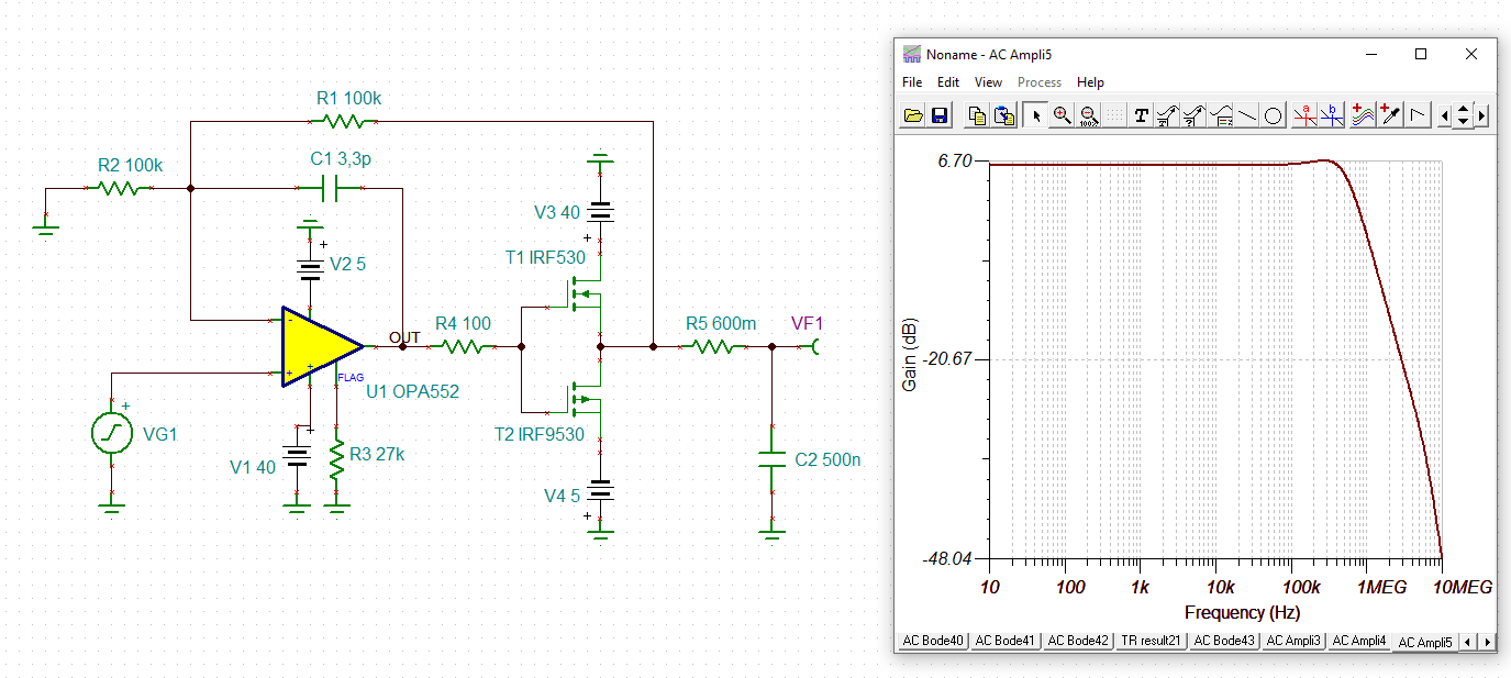
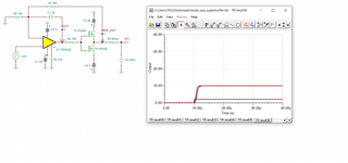
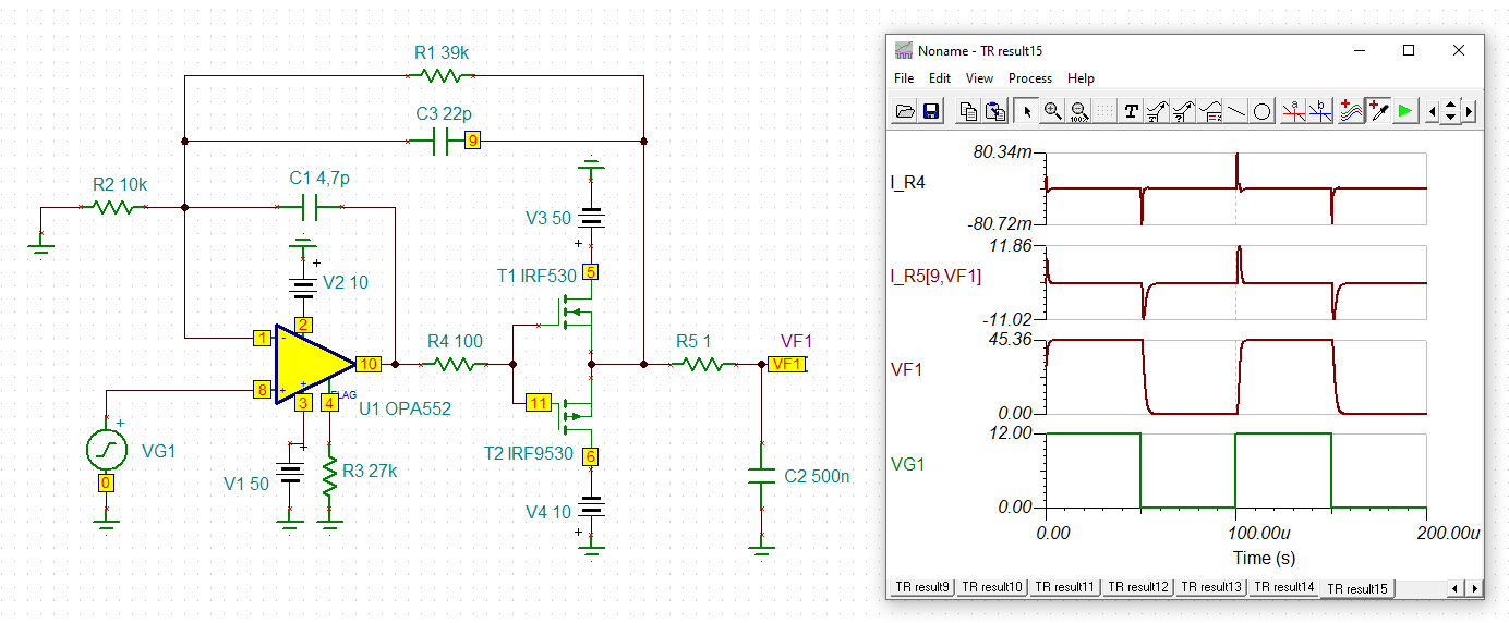
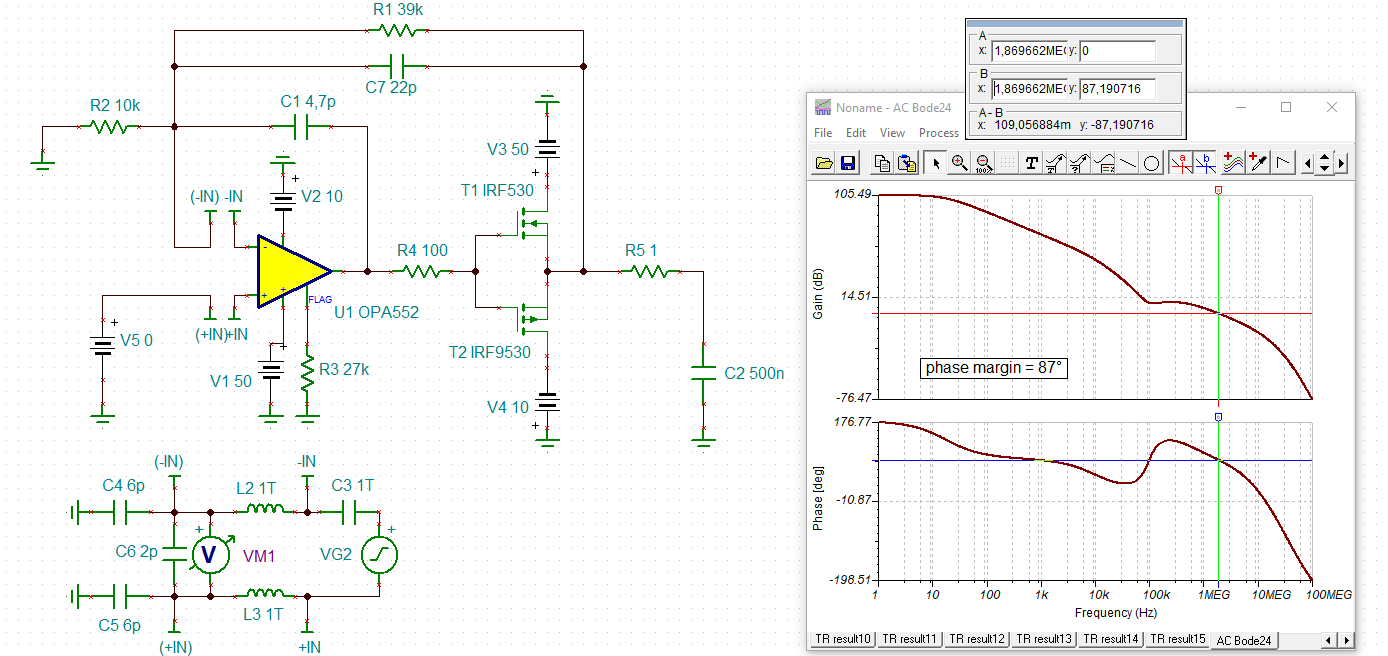
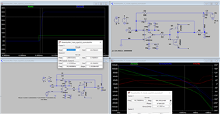
g ltspice, slew rate for 500n is about 19v/us and PM is about 68deg. any comments on this?

  • Hi Tarun,

    but with Ltspice, it shows like expected. don't know why it is so

    I don't think that everything is ok. Measure the voltage between the inputs of OPA552. It should be zero. If not, the OPA552 is out ot regulation.

    And your modified circuit is not stable:

    tarun_opa552_6.TSC

    In your phase stability anaylsis is a mistake. You must look at the output of OPAmp not at the output of circuit.

    Again, something is wrong with the MOSFETs. Choose better MOSFETs and try again.

    Kai 

  • Hi Tarun,

    Below is the circuit's stability simulation (there was a typo in the simulated current boost circuit). The small AC signal point should be injected from the negative feedback node and not after the R4 and C1 LP filter (unless R4 is inside of the negative feedback loop from LTSpice simulation).  

    When performed in the transient step analysis, the following step responses are obtained, and it seems to be stable.  

    I do not know your specific rising/falling edge design requirements. OPA551 has a slew rate of 15V/usec and OPA552 has the slew rate of 24V/usec. If you want to have fast rising/falling response time, you may select the suitable op amps, also may require to select faster mosfets with lower gate to source capacitance. 

    If you have additional questions, please let us know. 

    Best,

    Raymond

  • Hi Raymond,

    Thanks for the suggestion. I will also try out some faster MOSFETs. could please send your simulation as I wasn't able to retrieve the same in my simulation. 

    B.R,

    Tarun

  • Hi kai and Raymond, i have updated the circuit. Looks like the mistake is that the source of Pmos should be connected to the source of Nmos in the simulation, so the reason we got weird results. although in the PCB it was right. Could you guys please confirm if the stability is good . 

    Also one more question, i had same exact setup on the PCB where gain=5, V+ = 43 and V- = 5 and with an input of 9V , the opamp broke. Is this because of the the power supplies were not enough? From 7 to 8 V as vin saturated at 34.3 around

    PwrBuffer_Slewrate.TSCpwrBuffer_usingkaiAnalysis.TSC

  • Hi Tarun,

    it was my mistake. In all my simulation files the PMOS is incorrectly connected with swapped drain and source connections. It happened because I saved the wrong file earlier and used it later without noticing the drawing mistake.

    Weirdly, I didn't notice the mistake, because in the phase stability analysis only the NMOS was turned-on all the time.

    Later, Raymond has noticed my mistake and informed me. Thanks Raymond for this!

    Appologies for my mistake, Tarun!

    Can you specify what you exactly mean by "the OPAmp broke"?

    When an OPAmp is instable it can start to oscillate and by this overheat. This can result in total damage. Did this happen?

    Also, what signal do you exactly want to apply to the output cap?

    If it is going all the way down to 0V, you might need to increase the negative supply voltage from -5V to -10V or so.

    I will look at your files and run your simulations.

    Kai

  • Hi kai,

    Can you specify what you exactly mean by "the OPAmp broke"?

    I checked if it is so heated up, but neither the opamp nor the transistor was heated up. so Opam has broken means the opamp wasn't responding to any input signal but nothing to look for the bare eye.

    When an OPAmp is instable it can start to oscillate and by this overheat. This can result in total damage. Did this happen?

    I didn't see any oscillation at the output. also attached is an oscilloscope image. also how my vin looks. (here vin (yellow signal) = around 3.8V, vout (green signal) = 18.6around V) .

    I thought I retrieved oscilloscope images for 8V input but the saving was not proper, it also looked like the attached image with same slope and no oscillations.

    If it is going all the way down to 0V, you

    you are right my vin goes all the way to exact 0v (if that is what you have asked)

    Let me know if any other questions.

    Thanks.

    B.R,

    Tarun

  • Hi Tarun,

    with 15pF the circuit will not be stable:

    tarun_opa552_10.TSC

    With 2pF the circuit looks better:

    This is another, probably even better way to stabilize the circuit, I think originally suggested by Raymond:

    Kai

  • Hi Tarun,

    sometimes the drain gate capacitance discharging into the output of OPAmp during steep edges at the output of OPAmp can damage the OPAmp's output stage. That's why I wanted to increase the gate resistor to 100R.

    I don't know what exactly killed your OPAmp. But it's always a good idea to have a stable circuit running without going into input or output saturation. That's why the phase stability analysis is so important.

    By the way, it's hard to believe that the OPA552 with its thermal shutdown was damaged due to overheating.

    How many OPAmp did brake? Maybe there's another cause for the damage?

    Kai

  • Hi Kai,

    That's why I wanted to increase the gate resistor to 100R.

    with 100ohm it looks unstable.

    How many OPAmp did brake?

    2 opamps already brake. that too at the same vin , looks like it's gonna happen, again (I couldn't figure out too). Although previously my opamp has VS-= -5V, would increase it to 10 and see if that's the cause.

  • Hi Raymond,

    Maybe there's another cause for the damage?

    could you help us out here?

    Can you specify what you exactly mean by "the OPAmp broke"?

    I checked if it is so heated up, but neither the opamp nor the transistor was heated up. so Opam has broken means the opamp wasn't responding to any input signal but nothing to look for the bare eye.

    When an OPAmp is instable it can start to oscillate and by this overheat. This can result in total damage. Did this happen?

    I didn't see any oscillation at the output. also attached is an oscilloscope image. also how my vin looks. (here vin (yellow signal) = around 3.8V, vout (green signal) = 18.6around V) .

    I thought I retrieved oscilloscope images for 8V input but the saving was not proper, it also looked like the attached image with same slope and no oscillations.

    If it is going all the way down to 0V, you

    you are right my vin goes all the way to exact 0v (if that is what you have asked)

    Let me know if any other questions.

    Thanks.

    B.R,

    Tarun

  • Hi kai,

    please find the latest phase and transient response circuits. Looks good. but my only question there is some deviation of the output voltage at VOPOUT, Is it normal or to be considered as the deviation larger for smaller vin. 

    PwrBuffer_Slewrate100r.TSCpwrBuffer_100r_usingkaiAnalysis.TSC    

  • Hi Tarun,

    after doing many many many simulations I would do it as follows:

    1. I would choose MOSFETs with low gate source capacitance. This will keep the erosion of phase margin accetably low and will enormously simplify the phase lead compensation.

    2. I would choose the OPA552 because it's faster than the OPA551.

    3. I would run the OPA552 at its minimum gain of about 5V/V.

    4. I would limit the gate currents of MOSFETs by the help of a suited current limiting resistor, even if this might complicate the phase lead compensation and might slow down the circuit. 

    5. As the parameters of MOSFETs can vary from lot to lot and from manufacturer to manufacturer, I would increase the headroom of phase margin by mounting an additional phase lead compensation. Keep in mind, that even if the simulation looks good, you may need some fine tuning with the final real world circuit.

    So, that's what I would do:

    tarun_opa552_14.TSC

    tarun_opa552_13.TSC

    I'm sorry, if this is not exactly what you wanted to hear.

    You are now prepared to carry out all necessary examinations to make your circuit run stably Relaxed

    Kai 

  • Hi Kai,

    I couldn't thank you enough. I will try out these in the actual hardware and see how it goes.

    I hope the opamp does not break. Grinning

    I wish you a pleasant weekend.

    Best Regards,

    Tarun 

  • Many thanks to Kai for his continuous and considerable efforts to assist Tarun with his OPA552 circuit stability and compensation questions. This e2e thread as been extensive and we should move to close it at this point.

    If additional questions arise once the actual circuit has been built and tested I suggest opening a fresh inquiry at that time.

    Regards, Thomas

    Precision Amplifiers Applications Engineering