- Ask a related questionWhat is a related question?A related question is a question created from another question. When the related question is created, it will be automatically linked to the original question.
This thread has been locked.
If you have a related question, please click the "Ask a related question" button in the top right corner. The newly created question will be automatically linked to this question.
Hello i am using the INA180B1 for an over current protection while charging an battery pack.
I simulated the circuit and it should work like expected
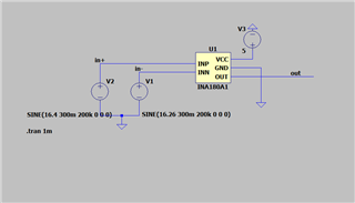
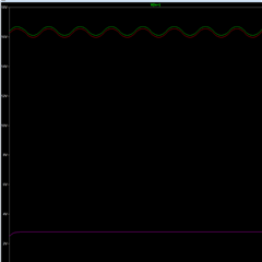
Green is the I+ signal, red the I- signal and pink the output of the INA180.
However the i dont get any output signal on my pcb from the INA. In my schematic have a an additional noise filter.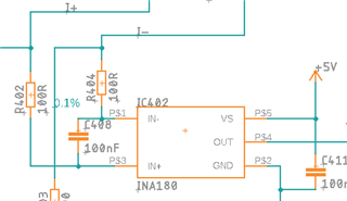
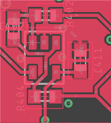
Here you can see my measurements with 200kHz switching frequency (dc Buck), 150mOHM shunt and 1A at my dc load.
pink is I+, yellow I- and blue is the INA Output.
As you can see, i only get the ringing as output but the 136mV difference are not amplified.
Thank you for your help
Hi Nassim,
your input filter has a corner frequency of 8kHz. This heavily suppress the 200kHz input signal. And why have you chosen the filter resistors higher than the recommended 10R?
Also, your signal frequency is too high for the INA180. A bandwidth of 350kHz means that the fundamental and all relevant harmonics of input signal must lie within 350kHz. I guess your input signal is no pure 200kHz sine?
And even if the input signal was a pure 200kHz sine, you will not have very much gain reserve. Figures 16, 17, 18 and 37 show how much the performance of INA180 is degraded at 200kHz.
Kai
Hi Kai,
I forget to say, that i desoldered the filter components and put in a jumper.
Originally i thought of getting a dc voltage and there wouldnt be any sine wave. But this is what comes out of my dc buck converter.
What would you recommend to do? Even if the gain is at 1, should the INA not then show me at least 136mV at the output?
Nassim
I am also wondering, why the simulation with the modeli downloaded from the INA180 page workes fine?
It has also a 200kHz signal.
Nassim,
There are two pinouts. Do you have the correct one? Your layout has Pinout B. I would expect some output signal as you have a difference. The output near GND does not make sense to me.
Hey Javier,
yes i am sure that i have the INA180B1DBVT, at least if digikey did not wrote the wrong part number on the package they delivered.
I also tried an other INA180B1, but all of them and not working with this signal.
Yesterday i had the chance to improve my dc buck output signal, so its not so noisy anymore, however the problem remains.
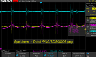
I'm reaching the point where even my electrical-engineer-skill-based toolbox is not taking my anywhere
Hi Nassim,
I would built a small, simple and separate test circuit and check with a true DC voltage source of 16VDC (no switcher supply!), a 150mR shunt and a resistive load wether the INA180 works at all and is able to produce an output voltage differing from 0V.
And I would desolder the INA180 from your board and check with an Ohmmeter for short circuits and other board damages.
Divide and conquer!
Kai
Hello Nassim,
I agree with Kai.
Output pin
The one thing I would look at in particular is the output pin. The reason I say this is that the output is always around ground. If you are willing unsolder pin 4 (output) from your board and verify if something on your board is loading the output. Measure on Pin 4 directly. I don't think for initial debug you need Scope as you should see a DC signal at the output.
Checking inputs
Place a resistor R402 and R404 back on the board and verify that you have about 90µA running through them by measuring the voltage drop across them. This will ensure that the input stage is on and working. I got 90µA from estimating figure 20 of datasheet and assuming 16VCM. With Vsense = 0 they both should draw that much current. Once you place a Vsense above 0mV those currents will imbalance.
Hey Kai, hello Javier,
thank you for your responses.
I measured the voltage over the two 100Ohm resistors and it was 8.2mV, so i think 82uA is close to 90uA as Javier estimated.
I checked the resistance and it is 377k to GND, so there should be no issue.
I also desoldered the INA and put a voltage from 1-5VDC on the pin. My fluke 177 says there is 1mA floating, but for me this is just saying, nothing is puling down my voltage.
Next i build a circuit with just the INA an 100mOhm Shunt and the 100nF at the 5VDC.
I have a Vin of 13,5VDC(my 102,5ohm was already at the limit) and could measure a 120mA current while i had a voltage drop of 12mV at the Shunt. But still the INA180 B1IDBVT remaind silent at the output pin.
So now i was sceptical, if the ic has really the B-Pinout. I took a brand new IC out and this is what i measured.

What is suprises me is, that i have 2,58kOhm between pin 1 and 3.
Does this seems correct to u?
Wish u a good weekend.
Nassim
Hi Nassim,
resistance measurements at a non-powered chip can show very misleading results. I know that one is tempted to do that, but I did fail so many times when doing that in the past, that I no longer do it.
Also, make no mistake, the INA180 is far away from being a simple differential amplifier. Don't overlook the small box called "bias" in figure 46 of datasheet. This box is the heart of an ultra high sophisticated chip. The internal circuit is secret and helps to make the chip being immune against common mode voltages heavily exceeding the supply voltage of INA180. And it allows to run the INA180 with an awesomely high common mode rejection. The INA180 seems to be tiny, but it can perform miracles...
Kai
Hello Nassim,
Kia is correct about about the input bias circuit and I have a method for you to verify an unpowered pinout. I think if you have IB at the input the inputs are correct and normally working correctly. I am worried if something is damaged at the output. Is there any capacitance or transient loading. If the ESD diodes are damaged and create a short that could be an issue on the output. Can you look at ESD diodes of unused part and part that is not working?
There are ESD protection diodes that protect the Output pin from being above VS and below GND. You the inputs have protection but are different. The ESD connection I highlighted can be used to verify the pinout. Make sure you use low current and device not powered on or on a board. Normally a diode checker on an handheld or DMM can be used.
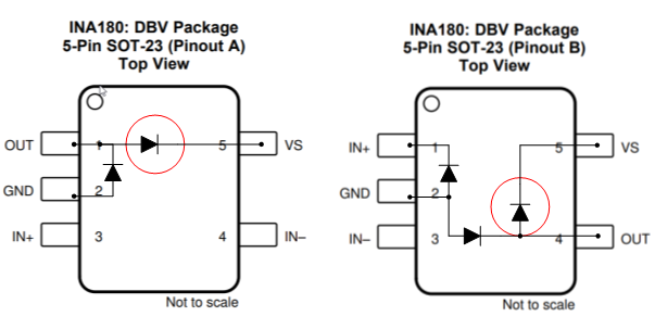
Hello Javier,
thank you for this information. I hope you had a good weekend.
As you said, i measured the diodes with my DMM and got the following results:
Is it normal, that the diode between VS and OUT is conductive in both directions? This seems off to me.
Nassim
I took a brand new INA180 out placed it on a proto board and attached a 100nF and 100mOhm to it.
VCC = 5V
VIN = 16V
ILOAD = 1A
VOUT = No output
i will try to get new INA180B1, because if i don't solder to hot i dont know what the problem could be....


Hi Nassim,
looks like you have "cold" solder joints. Add more flux and stay a bit longer with the solder tip on the solder joint. Wire terminals should see 350°C, but the SMD chip only 300°C maximum. If at all, then touch the chip terminals not directly at the package. Best only touch the solder pad and let the solder tin flow onto the chip terminals. And use lots of flux (e.g. FL88 from EDSYN).
I would take a wired 100nF cap. It's difficult to solder a SMD cap diretly at the terminals with a solder iron without destroying it. And I would think about using leaded tin for the experimenting.
Kai
Hello Nassim,
Did you try the diode check on a new device? Let me know the results after you attempt with a new device for diodes and the above test.