


Understanding Key Parameters for Audio Operational Amplifiers
There are a number of design considerations to take into account when designing your audio system. When choosing the right audio amp, here are some of the most important parameters to keep in mind.
Bandwidth and quiescent current
Bandwidth is the frequency range where the voltage gain of the amplifier is above the -3dB cutoff point of its maximum output value. For instance, if the maximum gain for an amplifier was given to be 50dB, and the operating frequency was at the bandwidth, then you would expect the maximum gain to now be 47dB and fall as the operating frequency increases.
The higher the bandwidth, the higher the operating frequency can be. Bandwidth and quiescent current are typically related to each other. In general, the higher the gain bandwidth, the higher the quiescent current. This is because the bandwidth is already related to the transconductance of the transistor. If you increase the drain current or the collector current of your transistor (ie increase the quiescent current) then the transconductance increases along with the overall bandwidth. Below are the transistor equations for bipolar and CMOS for a more visual representation:
![]()
Figure 1: Bipolar and MOSFET bandwidth equations
You can also see here that for the same quiescent current, bipolar op amps will have a higher bandwidth as transconductance rises with a linear increase in collector current. However, the higher the quiescent current, the more power dissipation one can expect. Having a higher bandwidth will help with high speed electronics, but having a high quiescent current will increase power usage which needs to be considered for battery powered systems.
Slew rate is also discussed when speed is a factor. The slew rate is often referred to as the maximum rate of change of an op amp's output voltage when a change occurs in the input, usually measured by V/us. The faster the slew rate, the faster the device. This parameter is also related to quiescent current.
Offset voltage and input bias current
Offset voltage is the differential input voltage needed to have zero volts in the output of your op amp. This offset is caused by differences in the differential pair of transistors. It is often treated as a DC source in the input. Offset drift is a function of temperature. At room temperature, it should be zero, but at temperatures deviating from room temperature, you will get more offset voltage. Digital circuits are often times integrated within op amps to cut down the offset voltage, but this comes at the expense of bandwidth.
Input bias current is also known as offset current. It comes from the current difference in the bases of the differential pair of the transistors. For FET devices, the gate resistance is normally so high, that this bias current comes from protection diode leakage. Regardless, they are modeled as current sources connected to each input. Resistances connected to either differential of the op amp can therefore generate an unwanted voltage whenever the op amp is being used in a noninverting mode.
Either parameter takes away from the overall precision of your op amp, so if precision is key for a design, choose products that have low offset voltages and low input bias currents.
Total Harmonic Distortion
Many designers also care about total harmonic distortion. While there is a specific THD value for every frequency within the audio range (20Hz-20kHz). Most datasheets will emphasize the THD at 1KHz for a good representation of the audio range as it is at the flat band component of the audio spectrum. Most data sheets however will also include data for a specified frequency range.
Total harmonic distortion is the sum of all the harmonics of a input signal present in the product's output. This normally sounds like additional tones in addition to the input signal. If the input was say 1kHz, non-linearities through real devices produce integer multiples at 2kHz (second harmonic), 3kHz (third harmonic) and so on and so forth. Therefore, lower THD is a closer representation of the input signals as there is less interference. THD is calculated by this formula:
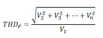
Where Vn on the top is the voltage at the nth harmonic. THD is sometimes measured in decibels as well.
Noise Parameters
Having a low noise amplifier is very important for lower frequency applications like preamplification. Noise is normally measured by voltage and current fluctuations at the input of an amplifier. Voltage noise fluctuation is tested with shorted inputs while current fluctuations are measured with open inputs. In either case both are measured in nanoamps or nanovolts per square root frequency. Typically, like THD, the 1kHz noise is normally chosen for representation.
There are a number of factors that influence the amount of noise present for an amplifier including the temperature, the internal makeup of the amplifier, bandwidth, external impedance of the inputs of the amplifier, and more.
Many op amps will have external resistors for gain control, so it's important to know that these external resistors add to the overall noise. External resistance noise can be calculated by this equation:
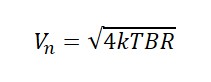
Where k is the Boltzmann constant, T is the temperature in Kelvin, B, is the bandwidth or frequency of operation.
Input current noise varies a lot more than input voltage noise from femtoamps to picoamps which is another reason why input voltage noise is usually shown primarily on the datasheet. The discrepancy normally comes from the architecture of the op amp. For BJT and JFET architectures, the current noise is the shot noise which comes from the bias current and universal charge constant.

The current noise will interact with source resistance to create a input voltage noise that could be more than the designer anticipated.
Input noise voltages from other sources are added together in a root sum of squares and don't have a simple way of calculation since it's a culmination of a plethora of sources. However, it's important to be mindful that depending on your design, the input voltage noise could be greatest from external resistances, input current noise reacting with source resistances, or internal input voltage noise specific to the architecture of your op amp.
